In short, ion beam sputtering is used to create exceptionally high-quality thin films for demanding applications. Its most common uses are in the manufacturing of precision optics, advanced semiconductors, laser components, and high-stability sensors like gyroscopes. This is because the process offers unparalleled control over film properties, resulting in layers that are incredibly dense, uniform, and strongly bonded to their substrate.
Ion beam sputtering (IBS) is not a general-purpose coating method. It is a specialist process chosen when the absolute highest film density, adhesion, and uniformity are non-negotiable, particularly for advanced optical and electronic components where material performance is critical.
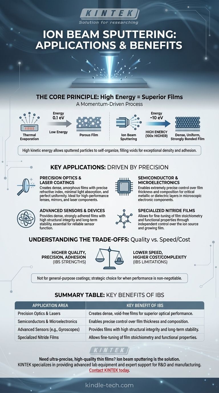
The Core Principle: Why High Energy Creates Superior Films
The unique applications of ion beam sputtering are a direct result of its underlying physics. Unlike other methods, it uses a highly controlled, high-energy process to deposit material atom by atom.
A Momentum-Driven Process
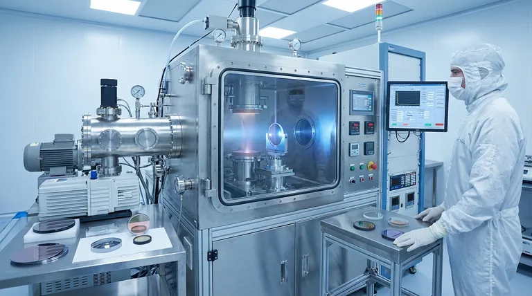
At its core, IBS uses a focused beam of ions to bombard a solid target material. This impact has enough momentum to physically knock atoms or molecules off the target, "sputtering" them towards a substrate where they form a thin film.
The High-Energy Advantage
Sputtered particles from an IBS system have an average energy of around 10 electron volts (eV). This is approximately 100 times higher than the energy of particles deposited through thermal evaporation methods.
Superior Adhesion and Density
This high kinetic energy is the key. When the energetic particles land on the substrate, they don't just "stick" where they land. They have enough mobility to migrate across the surface, finding ideal lattice sites and filling in microscopic voids.
This self-organizing action results in films that are exceptionally dense, uniform, and firmly bonded to the substrate, with minimal internal stresses or defects.
Key Applications Driven by Precision
The physical properties achieved through IBS make it the ideal choice for applications where material imperfection leads to failure.
Precision Optics and Laser Coatings
Applications like high-performance lenses, mirrors, and laser bar coatings demand films with a precise refractive index, minimal light absorption, and perfect uniformity. IBS excels here because it can create dense, amorphous optical films with virtually no voids, which would otherwise scatter light and degrade performance.
Semiconductor and Microelectronics
In semiconductor fabrication, IBS is used to deposit specific metallic or dielectric layers. The process's monoenergetic and highly collimated ion beam allows for extremely precise control over film thickness and composition, which is critical for the function of microscopic electronic components.
Advanced Sensors and Devices
Devices like high-performance gyroscopes rely on components with perfectly stable and uniform material properties over time. The dense, strongly adhered films created by IBS provide the structural integrity and stability required for these sensitive instruments to function reliably.
Specialized Nitride Films
The versatility of IBS allows it to sputter a wide range of materials, including those needed to form durable and functional nitride films. The independent control over the ion source and the growing film allows for fine-tuning of the film's stoichiometry and properties.
Understanding the Trade-offs
No technology is without its limitations. The precision of IBS comes with important considerations.
Lower Deposition Rate
The meticulous, atom-by-atom deposition process is inherently slower than bulk coating methods like thermal evaporation or conventional magnetron sputtering. The focus is on quality over quantity.
System Complexity and Cost
An ion beam sputtering system, with its dedicated high-voltage ion source and control mechanisms, is more complex and expensive to build and operate than simpler deposition technologies.
Not for General-Purpose Coating
Because of its slower speed and higher cost, IBS is not a practical choice for applications where the primary drivers are speed and low cost, such as decorative coatings or simple protective layers.
Making the Right Choice for Your Goal
Selecting a deposition method requires aligning the technique's strengths with your project's primary objective.
- If your primary focus is creating high-performance optical coatings: IBS is the superior choice due to its ability to produce dense, uniform films with precise and stable optical properties.
- If your primary focus is fabricating advanced semiconductors or sensors: The exceptional control over film thickness, density, and adhesion offered by IBS is essential for device performance and reliability.
- If your primary focus is speed and cost for general-purpose coatings: You should evaluate simpler methods like thermal evaporation or magnetron sputtering, as IBS may be unnecessarily complex and slow.
Ultimately, selecting ion beam sputtering is a strategic decision to prioritize film quality and precision above all other factors.
Summary Table:
| Application Area | Key Benefit of IBS |
|---|---|
| Precision Optics & Lasers | Creates dense, void-free films for superior optical performance. |
| Semiconductors & Microelectronics | Enables precise control over film thickness and composition. |
| Advanced Sensors (e.g., Gyroscopes) | Provides films with high structural integrity and long-term stability. |
| Specialized Nitride Films | Allows fine-tuning of film stoichiometry and functional properties. |
Need ultra-precise, high-quality thin films for your critical application?
Ion beam sputtering is the solution when the highest film density, adhesion, and uniformity are non-negotiable. At KINTEK, we specialize in providing the advanced lab equipment and expert support needed to achieve these demanding specifications.
Our solutions are tailored for laboratories focused on R&D and manufacturing in optics, semiconductors, and sensor technology.
Contact KINTEK today to discuss how our ion beam sputtering expertise can enhance your project's success.
Visual Guide
Related Products
- Electron Beam Evaporation Coating Gold Plating Tungsten Molybdenum Crucible for Evaporation
- Electron Beam Evaporation Coating Oxygen-Free Copper Crucible and Evaporation Boat
- Electron Beam Evaporation Coating Conductive Boron Nitride Crucible BN Crucible
- E Beam Crucibles Electron Gun Beam Crucible for Evaporation
People Also Ask
- What is the voltage of e-beam evaporation? Achieve Precise Thin-Film Deposition
- What materials are used in electron beam evaporation? Master High-Purity Thin Film Deposition
- What are the applications of e-beam evaporation? Achieve High-Purity Coatings for Optics & Electronics
- What is the container that holds the metal source material called in e-beam evaporation? Ensure Purity and Quality in Your Thin-Film Deposition
- What is the process of e-beam coating? Achieve High-Purity, Precise Thin Films for Your Lab


