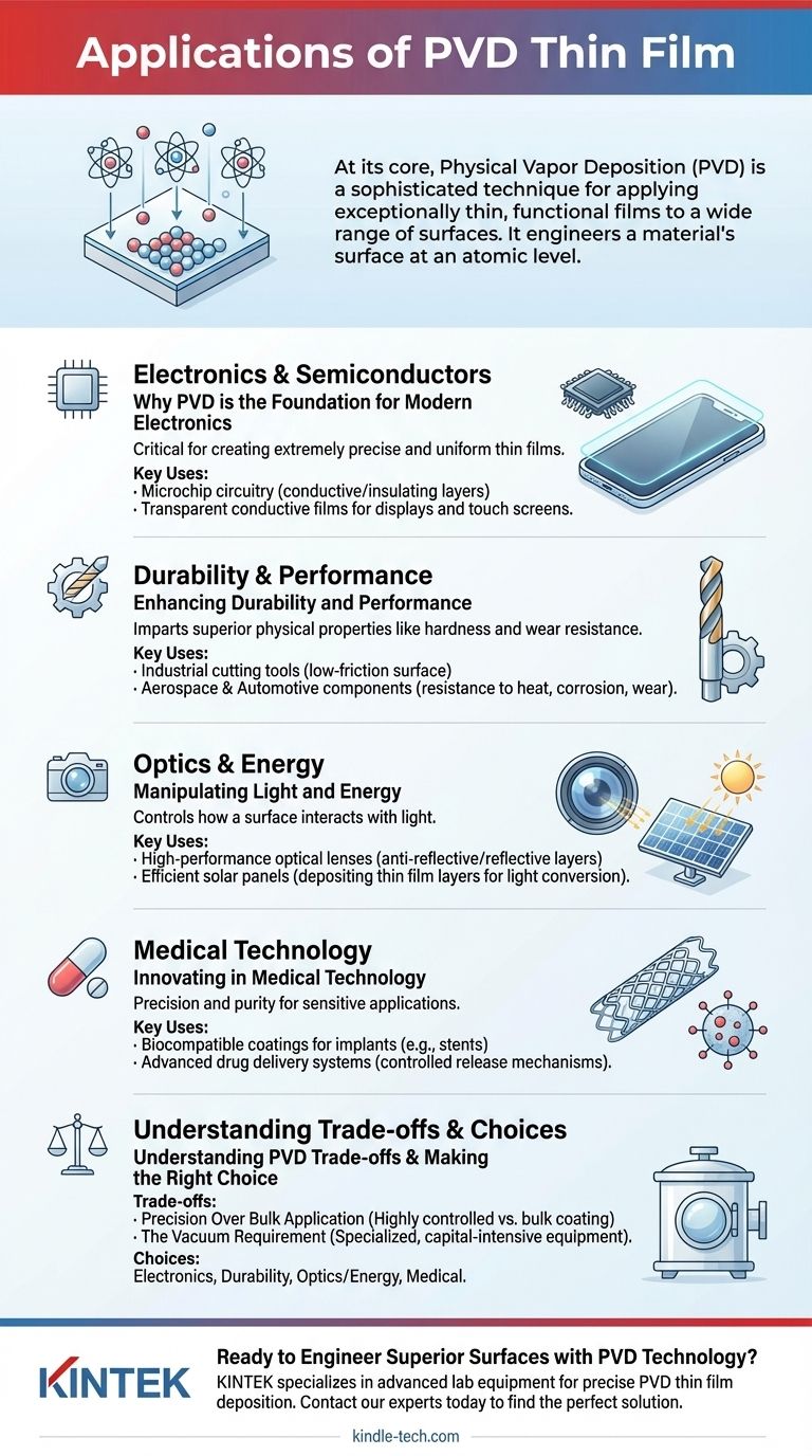
At its core, Physical Vapor Deposition (PVD) is a sophisticated technique for applying exceptionally thin, functional films to a wide range of surfaces. Its applications are incredibly diverse, spanning from the construction of microchips and semiconductor devices to creating durable protective layers for cutting tools, advanced optical coatings for lenses, and biocompatible layers for medical implants.
PVD is not merely a coating; it is a fundamental manufacturing process that precisely engineers a material's surface at an atomic level. This control is the reason PVD is essential for creating the high-performance properties required by modern electronics, optics, and medical technology.

Why PVD is the Foundation for Modern Electronics
PVD processes, particularly sputtering, are critical in electronics because they allow for the creation of extremely precise and uniform thin films. This level of control is non-negotiable for building the microscopic structures that power our digital world.
Creating Microchips and Semiconductors
In the semiconductor industry, PVD is used to deposit the ultra-thin layers of conductive or insulating materials that form the intricate circuitry of a microchip. The process ensures that each layer has the exact thickness and composition required for the device to function correctly.
Powering Displays and Touch Screens
The transparent conductive films on the screen of your mobile phone, laptop, or tablet are often created using PVD. These layers must be thin enough to be invisible yet conductive enough to register your touch, a balance that PVD achieves with high precision.
Enhancing Durability and Performance
One of the most common industrial uses for PVD is to impart superior physical properties—like hardness and wear resistance—to a substrate material.
For Industrial Cutting Tools
PVD coatings are applied to cutting tools and drills to create an exceptionally hard, low-friction surface. This dramatically increases the tool's lifespan, reduces wear, and improves its performance in demanding manufacturing environments.
In Aerospace and Automotive Components
In industries where components are subjected to extreme stress and friction, PVD provides a durable protective layer. These coatings can improve resistance to heat, corrosion, and wear, which is critical for the reliability of aerospace and automotive parts.
Manipulating Light and Energy
PVD gives manufacturers the ability to control how a surface interacts with light, leading to significant advancements in optics and renewable energy.
Crafting High-Performance Optical Lenses
Optical coatings on lenses for cameras or eyeglasses are designed to manage reflection and transmission. PVD is used to apply these anti-reflective or reflective layers with extreme precision, enhancing the performance of the optical device.
Building Efficient Solar Panels
Solar cells are built from multiple layers of different materials, each with a specific function in converting sunlight into electricity. PVD is a key method for depositing some of these thin films, contributing to the panel's overall efficiency.
Innovating in Medical Technology
The precision and purity of PVD films make them ideal for sensitive medical applications where biocompatibility and advanced functionality are paramount.
Coating Medical Implants
PVD is used to apply biocompatible coatings to implants like stents. These thin films can be loaded with microscopic layers of medication designed for a slow, controlled release directly into the bloodstream.
Enabling Advanced Drug Delivery
The technology is also being leveraged to develop novel drug delivery systems. PVD can create ultra-small structures capable of delivering powerful anti-cancer drugs in extremely precise, targeted amounts.
Understanding the Trade-offs of PVD
While powerful, the PVD process is highly specialized and is not a universal solution for all coating needs. Understanding its nature is key to appreciating its applications.
Precision Over Bulk Application
PVD is fundamentally a precision process. It excels at creating highly controlled, uniform, and functional thin films for advanced devices. It is less suited for simple, bulk coating where cost is the primary driver and precision is secondary.
The Vacuum Requirement
PVD methods like sputtering and evaporation must occur in a high-vacuum environment. This requires specialized, capital-intensive equipment, positioning it as an advanced industrial process rather than a simple workshop technique.
Making the Right Choice for Your Goal
The decision to use PVD is driven entirely by the specific surface properties you need to achieve.
- If your primary focus is electronics and semiconductors: PVD is the industry standard for depositing the ultra-thin, uniform conductive and insulating layers required for micro-fabrication.
- If your primary focus is mechanical durability: PVD provides hard, low-friction coatings that dramatically extend the life and improve the performance of industrial tools and components.
- If your primary focus is advanced optics or energy: PVD offers the precise control needed to engineer how a surface reflects, refracts, or absorbs light for high-performance lenses and solar cells.
- If your primary focus is medical innovation: PVD enables the creation of biocompatible surfaces and sophisticated drug-delivery mechanisms on medical implants and devices.
Ultimately, PVD is the enabling technology that transforms an ordinary surface into a high-performance, functional component.
Summary Table:
| Application Area | Key PVD Uses | Primary Benefit |
|---|---|---|
| Electronics & Semiconductors | Microchip circuitry, transparent conductive films | Extreme precision, uniformity for device functionality |
| Industrial Durability | Cutting tools, aerospace/automotive components | Superior hardness, wear resistance, and longevity |
| Optics & Energy | Anti-reflective lenses, solar panel layers | Precise control of light reflection/transmission |
| Medical Technology | Biocompatible implant coatings, drug delivery systems | High purity, controlled release, and biocompatibility |
Ready to Engineer Superior Surfaces with PVD Technology?
KINTEK specializes in advanced lab equipment and consumables for precise PVD thin film deposition. Whether you're developing next-generation microchips, durable industrial tools, high-performance optics, or innovative medical devices, our solutions deliver the exact surface properties you need.
We help you:
- Achieve atomic-level precision for your most demanding applications.
- Enhance product durability, efficiency, and functionality.
- Leverage industry-leading technology for R&D and production.
Let's discuss your project. Contact our experts today to find the perfect PVD solution for your laboratory's specific challenges.
Visual Guide
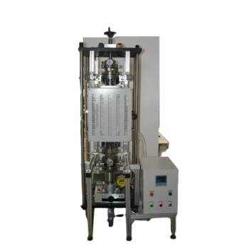
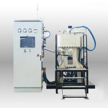
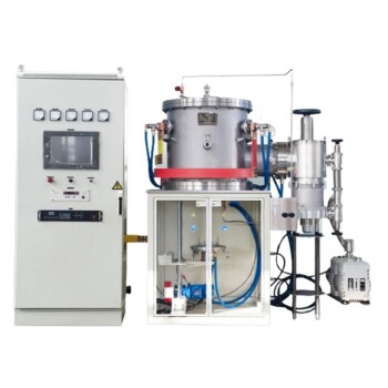
Related Products
- RF PECVD System Radio Frequency Plasma-Enhanced Chemical Vapor Deposition RF PECVD
- Split Chamber CVD Tube Furnace with Vacuum Station Chemical Vapor Deposition System Equipment Machine
- Chemical Vapor Deposition CVD Equipment System Chamber Slide PECVD Tube Furnace with Liquid Gasifier PECVD Machine
- VHP Sterilization Equipment Hydrogen Peroxide H2O2 Space Sterilizer
- Vacuum Hot Press Furnace Heated Vacuum Press Machine Tube Furnace
People Also Ask
- What is the principle of plasma enhanced chemical vapor deposition? Achieve Low-Temperature Thin Film Deposition
- What is an example of PECVD? RF-PECVD for High-Quality Thin Film Deposition
- What are the applications of PECVD? Essential for Semiconductors, MEMS, and Solar Cells
- How does RF power create plasma? Achieve Stable, High-Density Plasma for Your Applications
- Why does PECVD commonly use RF power input? For Precise Low-Temperature Thin Film Deposition