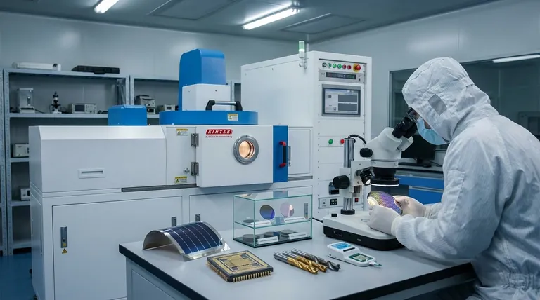
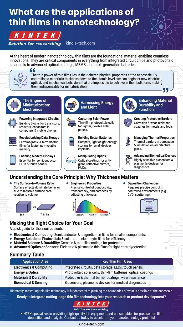
At the heart of modern nanotechnology, thin films are the foundational material enabling countless innovations. They are the critical components in everything from integrated circuit chips and photovoltaic solar cells to advanced optical coatings, micro-electromechanical systems (MEMS), and next-generation batteries.
The true power of thin films lies in their altered physical properties at the nanoscale. By controlling a material's thickness down to the atomic level, we can engineer new electrical, optical, and mechanical behaviors that are impossible to achieve in their bulk form, making them indispensable for miniaturization.
The Engine of Miniaturization: Electronics
Thin films are the bedrock of the entire semiconductor industry, allowing for the continuous miniaturization that drives modern computing.
Powering Integrated Circuits
Nearly all modern electronics rely on thin films. They are used to build the transistors, resistors, and capacitors that make up the integrated circuit chips in our computers and mobile phones.
Revolutionizing Data Storage
Researchers are actively developing ferromagnetic and ferroelectric thin films. These materials promise to create non-volatile computer memory that is faster and more energy-efficient than current technologies.
Enabling Modern Displays
Semiconductor thin films are essential for manufacturing light-emitting diodes (LEDs) and the touch panels used in virtually every smartphone and tablet.
Harnessing Energy and Light
By manipulating materials at the thin film level, we can control how they interact with energy, from photons to electrons.
Capturing Solar Power
Thin-film photovoltaic cells are a major application, allowing for the creation of lighter, more flexible, and potentially cheaper solar panels compared to traditional silicon wafers.
Building Better Batteries
Thin-film batteries offer a way to create incredibly compact and lightweight energy storage. This is critical for small electronic devices, medical implants, and sensors.
Manipulating Optics
Thin films are used as optical coatings to reduce glare on eyeglasses, create highly reflective mirrors, and power the head-up displays projected onto the windshields of modern cars.
Enhancing Material Durability and Function
Beyond electronics, thin films are applied to the surface of bulk materials to grant them entirely new properties.
Creating Protective Barriers
These films can act as a shield against the environment. They are widely used as protective coatings to prevent corrosion on metals or as wear-resistant layers on cutting tools.
Managing Thermal Properties
In the aerospace industry, thin films serve as thermal barriers on components exposed to extreme heat. In construction, they are used on architectural glass for thermal insulation.
Advancing Biomedical Devices
The unique properties of thin films make them ideal for creating highly sensitive biosensors and plasmonic devices, which can be used for rapid medical diagnostics.
Understanding the Core Principle: Why Thickness Matters
The revolutionary applications of thin films are not arbitrary; they emerge from a fundamental shift in material physics that occurs at the nanoscale.
The Surface-to-Volume Ratio
As a material becomes a thin film, its surface area becomes massive relative to its volume. This means that surface effects, which are negligible in bulk materials, begin to dominate the material's overall behavior.
Engineered Properties
This dominance of surface effects allows engineers to create materials with tailored properties. Electrical conductivity, optical transparency, and mechanical hardness can all be precisely controlled by adjusting the film's thickness and structure.
Deposition Challenges
The primary trade-off is manufacturing complexity. Creating a perfectly uniform, defect-free thin film is a significant engineering challenge. The methods used, like chemical vapor deposition or sputtering, require precise control in highly controlled environments.
Making the Right Choice for Your Goal
The specific type of thin film and its properties are chosen based on the intended technological outcome.
- If your primary focus is electronics and computing: You will utilize semiconductor and magnetic thin films to build smaller, faster, and more efficient components.
- If your primary focus is energy solutions: You will prioritize photovoltaic and solid-state electrolyte films to improve energy conversion and storage efficiency.
- If your primary focus is material science and durability: You will explore ceramic and metallic coatings for their unmatched protective properties against wear, corrosion, and heat.
- If your primary focus is advanced optics or sensors: You will investigate dielectric and plasmonic thin films to precisely control light or detect specific molecules.
Ultimately, mastering thin film technology is fundamental to pushing the boundaries of what is possible at the nanoscale.
Summary Table:
| Application Area | Key Thin Film Uses |
|---|---|
| Electronics & Computing | Integrated circuits, data storage, LEDs, touch panels |
| Energy & Optics | Photovoltaic solar cells, thin-film batteries, optical coatings |
| Materials & Durability | Protective & thermal barrier coatings, wear resistance |
| Biomedical & Sensing | Biosensors, plasmonic devices for medical diagnostics |
Ready to integrate cutting-edge thin film technology into your research or product development?
KINTEK specializes in providing high-quality lab equipment and consumables for precise thin film deposition and analysis. Whether you are developing next-generation electronics, energy solutions, or advanced materials, our expertise can help you achieve superior results.
Contact us today to discuss how our solutions can accelerate your nanotechnology projects!
Visual Guide
Related Products
- Aluminum-Plastic Flexible Packaging Film for Lithium Battery Packaging
- Thin-Layer Spectral Electrolysis Electrochemical Cell
People Also Ask
- How is aluminum foil utilized as a consumable during the assembly of cold sintering molds? Optimize Tooling Longevity
- How to tell if a lithium-ion battery is bad? Spot the critical signs of failure before it's too late.
- What is the thinnest coating? Unlocking Unique Properties at the Atomic Scale
- What are the three types of lamination? Choose the Perfect Finish for Your Print Project
- Is there a way to test lithium batteries? Understand Voltage vs. True Health

