At its core, Low-Pressure Chemical Vapor Deposition (LPCVD) is a highly refined process for creating exceptionally uniform and pure thin films, making it a cornerstone of modern microfabrication. While it shares the fundamental principles of all chemical vapor deposition (CVD) methods, its use of a vacuum environment provides distinct advantages for producing high-quality materials over large areas and complex topographies.
The crucial advantage of LPCVD is not just what it does, but how it does it. By reducing the chamber pressure, the process enables gas molecules to travel further and more freely, resulting in superior film uniformity and the ability to coat many substrates simultaneously with high purity.
How Low Pressure Changes Everything
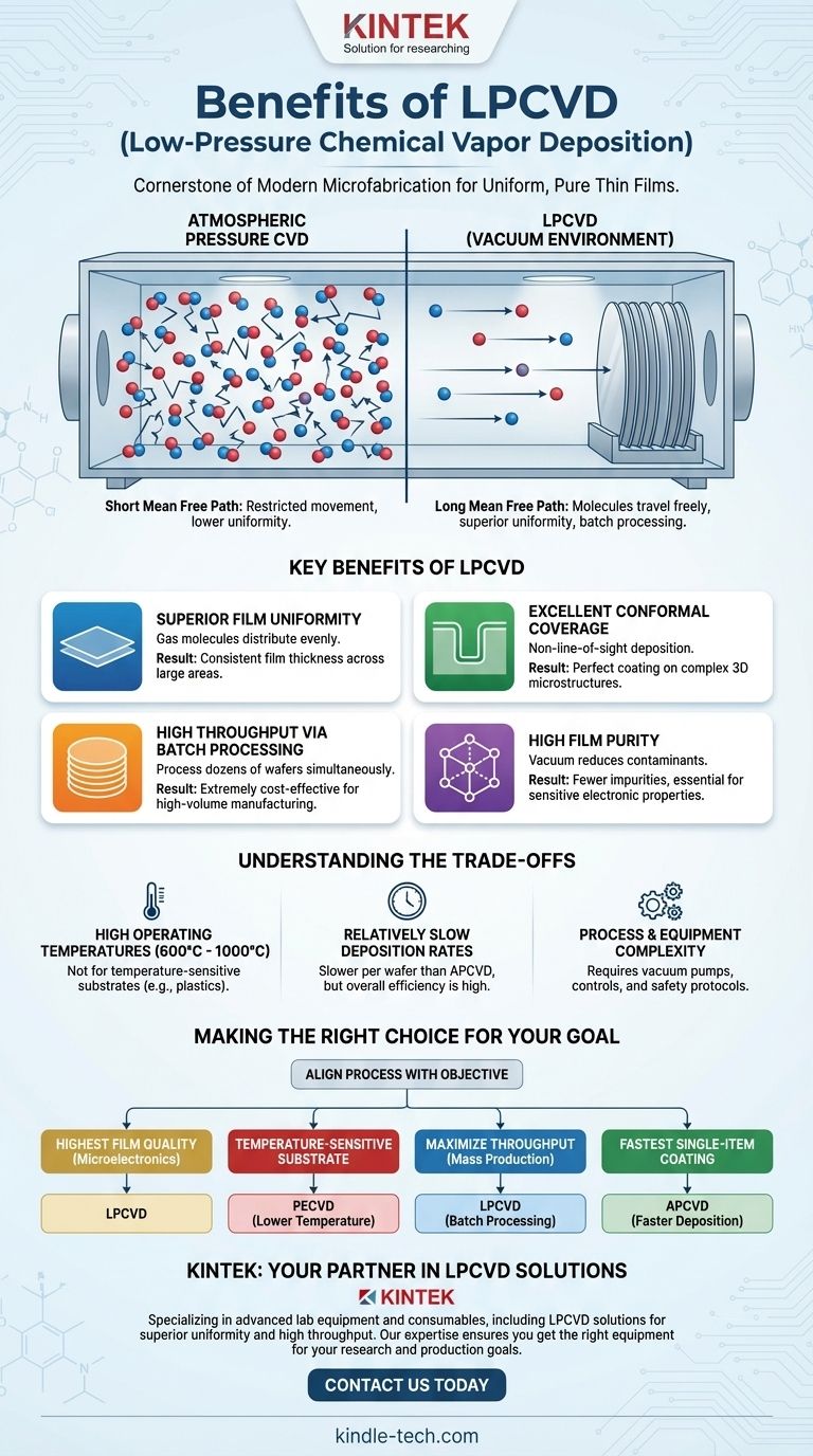
To understand the benefits of LPCVD, we must first understand the physics of operating in a vacuum. The key concept is the mean free path, which is the average distance a gas molecule travels before colliding with another.
The Role of Mean Free Path
In a standard atmospheric pressure system, the chamber is crowded with gas molecules that collide constantly. This restricts their movement.
In an LPCVD system, the pressure is reduced by a factor of 1,000 to 10,000. This drastically increases the mean free path, allowing precursor gas molecules to travel much farther before interacting. This single change is the source of LPCVD's primary benefits.
Key Benefits of the LPCVD Process
The unique environment inside an LPCVD reactor directly translates into tangible advantages for manufacturing, particularly in the semiconductor industry.
Superior Film Uniformity
Because gas molecules can travel long distances without collision, they distribute themselves very evenly throughout the reaction chamber.
This leads to a highly uniform deposition rate across the entire surface of a substrate. The resulting film has a consistent thickness, which is critical for the performance of electronic devices.
Excellent Conformal Coverage
The long mean free path also enables LPCVD to provide outstanding conformal coverage. This means the film perfectly conforms to the shape of complex, three-dimensional microstructures on a wafer.
Unlike line-of-sight deposition methods, the gas in LPCVD can find its way into deep trenches and around sharp corners, ensuring a continuous and uniform coating everywhere.
High Throughput via Batch Processing
The non-line-of-sight nature and high uniformity of LPCVD allow for incredible process efficiency. Instead of processing one wafer at a time, dozens or even hundreds of wafers can be stacked vertically in a "boat."
The precursor gases flow between the wafers, depositing material uniformly on all of them at once. This batch processing capability makes LPCVD extremely cost-effective for high-volume manufacturing.
High Film Purity
Operating under a vacuum inherently reduces the concentration of unwanted background gases and contaminants in the chamber.
This results in the growth of high-purity films, as there is a lower probability of incorporating impurities into the material. This is essential for achieving the desired electrical and material properties in sensitive applications.
Understanding the Trade-offs
No process is perfect. The benefits of LPCVD come with specific requirements and limitations that are critical to understand.
High Operating Temperatures
A significant drawback of many LPCVD processes is the need for high temperatures, often in the range of 600°C to 1000°C, to drive the necessary chemical reactions.
This high thermal budget restricts its use to substrates that can withstand such heat. It is not suitable for depositing films on temperature-sensitive materials like plastics or certain completed device layers.
Relatively Slow Deposition Rates
While the overall throughput is high due to batch processing, the actual rate of film growth on any single wafer is typically slower than atmospheric pressure CVD (APCVD).
The choice between them depends on whether the priority is speed for a single part or efficiency for a large batch.
Process and Equipment Complexity
LPCVD systems require vacuum pumps, sealed chambers, and sophisticated process controls to manage pressure and gas flow precisely. The precursor gases used are also often hazardous.
This makes the equipment more complex and expensive than simpler atmospheric systems and requires stringent safety protocols.
Making the Right Choice for Your Goal
Selecting a deposition method requires aligning the process capabilities with your primary objective.
- If your primary focus is the highest film quality for microelectronics: LPCVD is often the superior choice for its unparalleled uniformity, conformality, and purity on silicon wafers.
- If your primary focus is coating a temperature-sensitive substrate: LPCVD is unsuitable; a lower-temperature process like Plasma-Enhanced CVD (PECVD) would be necessary.
- If your primary focus is maximizing throughput for mass production: LPCVD's batch processing capability makes it one of the most efficient and scalable deposition technologies available.
- If your primary focus is the fastest possible coating on a single item: LPCVD's deposition rate is slower than other methods, so APCVD might be a better fit if batching is not an option.
Ultimately, choosing LPCVD is a strategic decision to prioritize film perfection and manufacturing scale over process speed and temperature flexibility.
Summary Table:
| Benefit | Key Feature | Ideal Use Case |
|---|---|---|
| Superior Film Uniformity | Consistent thickness across large areas | Microelectronics, semiconductor manufacturing |
| Excellent Conformal Coverage | Uniform coating on complex 3D structures | MEMS devices, advanced sensors |
| High Throughput | Batch processing of multiple wafers | High-volume production environments |
| High Film Purity | Reduced contamination in vacuum environment | Sensitive electronic applications |
Need high-quality thin films for your lab? KINTEK specializes in advanced lab equipment and consumables, including LPCVD solutions tailored for laboratories requiring superior uniformity and high throughput. Our expertise ensures you get the right equipment to meet your specific research and production goals. Contact us today to discuss how we can enhance your lab's capabilities!
Visual Guide
Related Products
- Inclined Rotary Plasma Enhanced Chemical Vapor Deposition PECVD Equipment Tube Furnace Machine
- Inclined Rotary Plasma Enhanced Chemical Vapor Deposition PECVD Equipment Tube Furnace Machine
- Chemical Vapor Deposition CVD Equipment System Chamber Slide PECVD Tube Furnace with Liquid Gasifier PECVD Machine
- Laboratory CVD Boron Doped Diamond Materials
- Microwave Plasma Chemical Vapor Deposition MPCVD Machine System Reactor for Lab and Diamond Growth
People Also Ask
- What is plasma activated chemical vapour deposition method? A Low-Temperature Solution for Advanced Coatings
- How does PECVD facilitate Ru-C nanocomposite films? Precision Low-Temperature Thin Film Synthesis
- How does the PECVD function enhance thin-film properties? Achieve Superior Chemical Stability & Durability
- How does plasma vapor deposition work? A Low-Temperature Coating Solution for Sensitive Materials
- What is the core value of PECVD compared to CVD? Discover the Low-Temperature Advantage for Thin-Film Coating
