At its core, Chemical Vapor Deposition (CVD) is a single process: using chemical reactions in a gas phase to deposit a solid thin film onto a substrate. The "different types" of CVD are not fundamentally different processes, but rather variations distinguished by the specific conditions—primarily pressure and the energy source—used to initiate and control that chemical reaction.
The crucial insight is that the choice between CVD methods is a strategic trade-off. You are primarily balancing the required deposition temperature against the desired film quality, deposition speed, and cost. Understanding how each method supplies energy to the precursor gases is the key to selecting the right one.
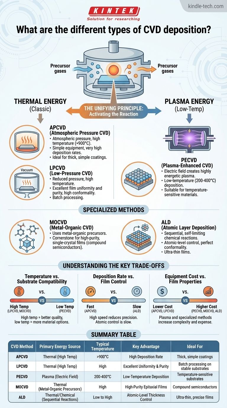
The Unifying Principle: Activating the Reaction
Every CVD process relies on providing enough energy to break down precursor gases and drive the chemical reaction that forms the thin film. The method used to supply this energy is the primary way we classify different CVD techniques.
Thermal Energy: The Classic Approach
The original and most straightforward method is to simply heat the substrate to a high temperature. The precursor gases decompose upon contact with the hot surface, initiating the deposition.
This thermal activation is the basis for the two most foundational CVD types.
APCVD (Atmospheric Pressure CVD)
This is the simplest form of CVD, conducted at normal atmospheric pressure. It is primarily driven by high temperatures (often >900°C).
Because it operates at atmospheric pressure, the equipment is relatively simple and the deposition rates are very high.
LPCVD (Low-Pressure CVD)
LPCVD operates under a vacuum, at reduced pressures. While still relying on high temperatures for the reaction, the low pressure significantly improves film uniformity and purity compared to APCVD.
The reduced pressure allows precursor molecules to travel further and coat complex, three-dimensional structures more evenly, a property known as conformality.
Plasma Energy: The Low-Temperature Solution
For substrates that cannot withstand high temperatures, like plastics or certain semiconductor devices, thermal energy is not a viable option. Plasma enhancement provides an alternative activation pathway.
PECVD (Plasma-Enhanced CVD)
In PECVD, an electric field is used to create a plasma (an ionized gas) within the chamber. This highly energetic plasma has enough power to break apart precursor gas molecules at much lower temperatures (typically 200-400°C).
This allows for the deposition of high-quality films on temperature-sensitive materials that would be damaged by traditional LPCVD or APCVD processes.
Specialized Methods for Advanced Materials
Some applications require exceptional crystal quality or atomic-level precision, leading to more specialized, and often more complex, CVD variants.
MOCVD (Metal-Organic CVD)
This technique uses metal-organic precursors, which are compounds containing both metal and carbon-hydrogen bonds. MOCVD is the cornerstone for creating high-purity, single-crystal films, particularly for compound semiconductors used in LEDs, lasers, and high-frequency electronics.
ALD (Atomic Layer Deposition)
While often considered a distinct process, ALD is a sub-class of CVD that offers the ultimate control. Instead of a continuous deposition, ALD builds the film one single atomic layer at a time through sequential, self-limiting chemical reactions.
This results in unparalleled precision, perfect conformality, and the ability to create ultra-thin films with angstrom-level thickness control.
Understanding the Key Trade-offs
Choosing a CVD method is never about finding a "best" option, but the right one for a specific goal. The decision involves navigating a few critical compromises.
Temperature vs. Substrate Compatibility
The most significant trade-off is deposition temperature. High-temperature processes like LPCVD produce excellent films but are incompatible with many materials. PECVD exists specifically to solve this problem, enabling deposition on a much wider range of substrates at the cost of more complex equipment.
Deposition Rate vs. Film Control
There is a direct inverse relationship between speed and precision. APCVD is extremely fast, making it ideal for thick, simple coatings where perfect uniformity isn't critical. At the other extreme, ALD is exceptionally slow but provides atomic-level control, essential for advanced microelectronics.
Equipment Cost vs. Film Properties
Simpler thermal methods like APCVD and LPCVD involve lower capital and operational costs. Introducing plasma (PECVD) or using highly specialized precursors and hardware (MOCVD, ALD) significantly increases the complexity and expense of the system.
Making the Right Choice for Your Goal
Your application's primary requirement will dictate the ideal CVD method.
- If your primary focus is high-throughput production of simple, thick films: APCVD is the most cost-effective choice due to its high deposition rate.
- If your primary focus is excellent film uniformity and purity on stable substrates: LPCVD offers a superior balance of quality and throughput for batch processing.
- If your primary focus is depositing films on temperature-sensitive materials: PECVD is the necessary choice, as it breaks the dependence on high thermal energy.
- If your primary focus is creating epitaxial (single-crystal) semiconductor films: MOCVD is the industry standard for applications like LEDs and advanced transistors.
- If your primary focus is absolute precision, conformality, and control over film thickness: ALD is the only method that can reliably deliver angstrom-level control.
By understanding that each CVD type is a tool optimized for a specific set of trade-offs, you can confidently select the right process for your technical and economic goals.
Summary Table:
| CVD Method | Primary Energy Source | Typical Temperature | Key Advantage | Ideal For |
|---|---|---|---|---|
| APCVD | Thermal (High Temp) | >900°C | High Deposition Rate, Simple Equipment | Thick, simple coatings, high throughput |
| LPCVD | Thermal (High Temp) | High (e.g., 500-900°C) | Excellent Uniformity & Purity | Batch processing on stable substrates |
| PECVD | Plasma (Electric Field) | 200-400°C | Low-Temperature Deposition | Temperature-sensitive substrates (e.g., plastics) |
| MOCVD | Thermal (Metal-Organic Precursors) | High | High-Purity Epitaxial Films | Compound semiconductors (LEDs, lasers) |
| ALD | Thermal/Chemical (Sequential Reactions) | Low to High | Atomic-Level Thickness Control | Ultra-thin, precise films with perfect conformality |
Still unsure which CVD method is right for your project? KINTEK specializes in lab equipment and consumables, serving laboratory needs. Our experts can help you navigate the trade-offs between temperature, speed, and cost to select the perfect CVD solution for your specific application—whether you need high-throughput APCVD or atomic-level precision with ALD. Contact our team today for a personalized consultation and unlock the full potential of your thin film processes!
Visual Guide
Related Products
- Chemical Vapor Deposition CVD Equipment System Chamber Slide PECVD Tube Furnace with Liquid Gasifier PECVD Machine
- Customer Made Versatile CVD Tube Furnace Chemical Vapor Deposition Chamber System Equipment
- HFCVD Machine System Equipment for Drawing Die Nano-Diamond Coating
- 915MHz MPCVD Diamond Machine Microwave Plasma Chemical Vapor Deposition System Reactor
- Split Chamber CVD Tube Furnace with Vacuum Station Chemical Vapor Deposition System Equipment Machine
People Also Ask
- What is plasma enhanced chemical vapor deposition PECVD equipment? A Guide to Low-Temperature Thin Film Deposition
- What types of substrates are used in CVD to facilitate graphene films? Optimize Graphene Growth with the Right Catalyst
- How are carbon nanotubes grown? Master Scalable Production with Chemical Vapor Deposition
- What are the advantages of chemical vapor deposition? Achieve Superior Thin Films for Your Lab
- What are the processes of vapor phase deposition? Understand CVD vs. PVD for Superior Thin Films


