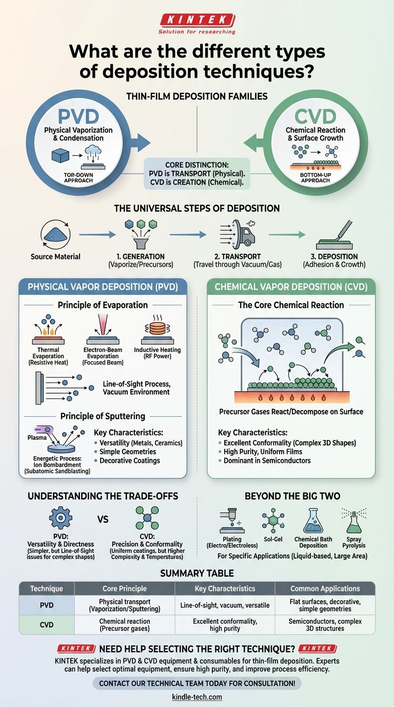
At the highest level, thin-film deposition techniques are categorized into two primary families: Physical Vapor Deposition (PVD) and Chemical Vapor Deposition (CVD). PVD involves physically vaporizing a solid source material in a vacuum and allowing it to condense onto a substrate, while CVD uses chemical reactions from precursor gases to grow a new material layer directly on the substrate's surface.
The core distinction lies in how the material travels and arrives. PVD is a physical process of transport, like spray-painting with atoms. CVD is a chemical process of creation, where a film is built atom-by-atom from reactive gases on the target surface.
The Universal Steps of Deposition
Before examining specific methods, it's useful to understand the fundamental sequence that most deposition techniques follow. This provides a framework for comparing different approaches.
From Source to Surface
Nearly every technique involves three stages:
- Generation: A source material is converted into a transportable species—either by vaporizing it (PVD) or by using volatile precursor gases (CVD).
- Transport: These species travel from the source to the substrate, typically through a vacuum or a controlled gas environment.
- Deposition: The species adhere to the substrate, forming a thin film and beginning the growth process.
Physical Vapor Deposition (PVD): A "Top-Down" Approach
PVD encompasses a family of methods that physically move material from a source (target) to a substrate. These processes occur under high or ultra-high vacuum conditions and do not involve chemical reactions to form the film.
The Principle of Evaporation
Evaporation is the most intuitive PVD method. A solid source material is heated in a vacuum until its atoms or molecules vaporize, travel in a straight line, and condense as a solid film on the cooler substrate.
There are several ways to heat the source material:
- Thermal Evaporation: Uses a simple resistive heat source (like a hot filament) to boil off the material.
- Electron-Beam Evaporation: A focused, high-energy beam of electrons heats the source material with great precision, allowing for the deposition of materials with very high melting points.
- Inductive Heating: Radio frequency (RF) power is used to induce eddy currents in a crucible, which in turn heats the source material inside it.
The Principle of Sputtering
Sputtering is a more energetic PVD process. Instead of boiling material off, it uses a plasma to bombard the source target with high-energy ions.
This bombardment acts like a subatomic sandblaster, knocking atoms loose from the target. These ejected atoms then travel and deposit onto the substrate, forming a dense and strongly adhered film.
Chemical Vapor Deposition (CVD): A "Bottom-Up" Approach
CVD is fundamentally different from PVD. It is a chemical process where the substrate is exposed to one or more volatile precursor gases, which react or decompose on the substrate surface to produce the desired film.
The Core Chemical Reaction
In a CVD process, reactant gases are introduced into a chamber containing the heated substrate. The thermal energy from the substrate provides the activation energy needed for chemical reactions to occur exclusively on its surface.
This process "grows" a high-purity, high-performance film directly on the wafer or component. Because it depends on gas flow and surface reactions rather than a direct line of sight, CVD is exceptionally good at creating uniform coatings.
Why CVD Dominates in Semiconductors
CVD is the most commonly used deposition method in the semiconductor industry. Its ability to produce extremely precise and conformal films—meaning they can coat complex, three-dimensional surface topographies evenly—is critical for manufacturing modern microelectronics.
Understanding the Trade-offs
The choice between PVD and CVD is dictated by the required film properties, the material being deposited, and the geometry of the substrate.
PVD: Versatility and Directness
PVD is often simpler and can be used to deposit a very wide range of materials, including metals and ceramics. However, because it's a "line-of-sight" process, it can struggle to coat complex shapes and undercut features uniformly.
CVD: Precision and Conformality
CVD excels at producing highly pure and uniform films that conform perfectly to the underlying surface. This precision comes at the cost of higher complexity, often requiring higher process temperatures and the handling of volatile and sometimes hazardous precursor chemicals.
Beyond the Big Two: Other Methods
While PVD and CVD are the dominant vapor-phase techniques, other chemical methods exist, often involving liquids. These include plating (electroplating and electroless), sol-gel, chemical bath deposition, and spray pyrolysis. These techniques are chosen for specific applications where vapor-based methods are impractical or unnecessary.
Making the Right Choice for Your Goal
Selecting the correct technique requires a clear understanding of your application's primary driver.
- If your primary focus is high-purity, uniform coatings on complex surfaces (like in semiconductors): CVD is the superior choice due to its excellent conformality and atomic-level precision.
- If your primary focus is depositing a wide range of metals or simple compounds onto a relatively flat surface: PVD techniques like sputtering or evaporation offer a versatile, direct, and often faster solution.
- If your primary focus is low-cost, large-area coating or a liquid-based process is required: Explore alternative chemical methods like plating or spray pyrolysis, which operate on entirely different principles.
Ultimately, understanding the fundamental difference between physical transport (PVD) and chemical creation (CVD) is the key to selecting the optimal deposition technique for your project.
Summary Table:
| Technique | Core Principle | Key Characteristics | Common Applications |
|---|---|---|---|
| PVD (Physical Vapor Deposition) | Physical transport of material via vaporization/sputtering | Line-of-sight, vacuum environment, versatile for metals/ceramics | Flat surfaces, decorative coatings, simple geometries |
| CVD (Chemical Vapor Deposition) | Chemical reaction of precursor gases on substrate surface | Excellent conformality, high purity, uniform coatings | Semiconductors, complex 3D structures, microelectronics |
Need help selecting the right deposition technique for your lab?
KINTEK specializes in laboratory equipment and consumables for thin-film deposition processes. Whether you're working with PVD systems for metal coatings or CVD setups for semiconductor applications, our experts can help you:
- Select the optimal equipment for your specific materials and substrate requirements
- Ensure high-purity results with our quality consumables and accessories
- Improve your deposition process efficiency and film quality
Let us help you achieve superior thin-film results. Contact our technical team today for personalized consultation!
Visual Guide
Related Products
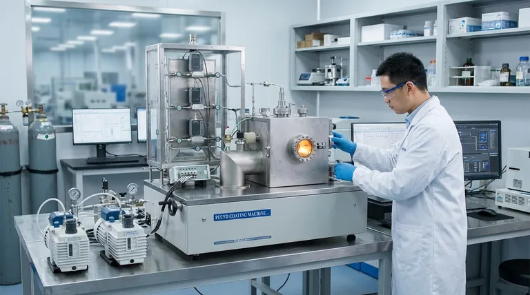
- Chemical Vapor Deposition CVD Equipment System Chamber Slide PECVD Tube Furnace with Liquid Gasifier PECVD Machine
- RF PECVD System Radio Frequency Plasma-Enhanced Chemical Vapor Deposition RF PECVD
- Microwave Plasma Chemical Vapor Deposition MPCVD Machine System Reactor for Lab and Diamond Growth
- Customer Made Versatile CVD Tube Furnace Chemical Vapor Deposition Chamber System Equipment
- 915MHz MPCVD Diamond Machine Microwave Plasma Chemical Vapor Deposition System Reactor
People Also Ask
- How expensive is chemical vapor deposition? Understanding the True Cost of High-Performance Coating
- What are the core advantages of PE-CVD in OLED encapsulation? Protect Sensitive Layers with Low-Temp Film Deposition
- Why is Chemical Vapor Deposition (CVD) equipment uniquely suited for constructing hierarchical superhydrophobic structures?
- What is plasma enhanced chemical vapor deposition PECVD equipment? A Guide to Low-Temperature Thin Film Deposition
- What is the chemical vapor deposition growth process? Build Superior Thin Films from the Atom Up


