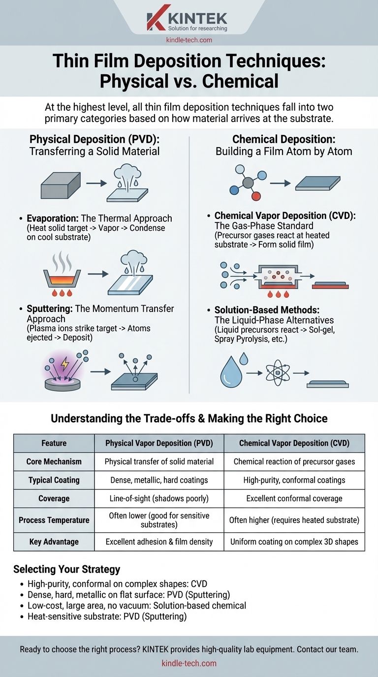
At the highest level, all thin film deposition techniques fall into two primary categories: Physical Deposition and Chemical Deposition. The core difference lies in how the film material arrives at the substrate. Physical methods physically transport a material from a solid source to the surface, while chemical methods use precursor chemicals that react to create a new, solid film directly on the surface.
The essential distinction is not which method is superior, but which mechanism is appropriate for the task. The choice between a physical or chemical process depends entirely on the desired film properties, the material being deposited, and the nature of the substrate.
The Two Pillars: Physical vs. Chemical Deposition
Every thin film deposition process begins with the same goal: to apply an exceptionally thin layer of material, often just a few atoms or molecules thick, onto a surface called a substrate. The method chosen to achieve this goal defines the film's characteristics, from its density and purity to how well it adheres to the surface.
The fundamental split in methodology—physical versus chemical—provides a clear framework for understanding your options.
Physical Vapor Deposition (PVD): Transferring a Solid Material
Physical Vapor Deposition (PVD) encompasses a family of processes that occur in a vacuum. The core principle is to take a solid source material, convert it into a vapor, and have it condense onto the substrate as a thin film.
Evaporation: The Thermal Approach
Evaporation is conceptually the simplest PVD method. A solid target material in a vacuum chamber is heated until it evaporates into a gaseous form. These gaseous atoms then travel through the vacuum and condense on the cooler substrate, much like steam fogging a cold mirror.
Sputtering: The Momentum Transfer Approach
Sputtering is a more energetic process. Instead of heat, it uses a plasma of an inert gas, such as argon. High-energy ions from this plasma are accelerated to strike the solid target material, physically knocking off or "sputtering" atoms. These ejected atoms then deposit onto the substrate, forming a dense and strongly adhered film.
Chemical Deposition: Building a Film Atom by Atom
Chemical deposition techniques do not start with the final film material in a solid form. Instead, they introduce precursor chemicals that undergo a reaction at or near the substrate, forming the desired film as a product of that reaction.
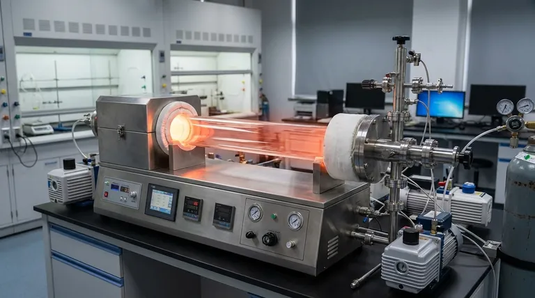
Chemical Vapor Deposition (CVD): The Gas-Phase Standard
In CVD, precursor gases are introduced into a reaction chamber containing a heated substrate. The heat provides the energy needed to trigger a chemical reaction between the gases, which results in the deposition of a high-purity solid film on the substrate's surface.
Solution-Based Methods: The Liquid-Phase Alternatives
This broad category includes techniques like sol-gel, spray pyrolysis, and chemical bath deposition. The unifying principle is the use of liquid chemical precursors instead of gases. These methods often operate at lower temperatures and do not always require a vacuum, making them potentially simpler and less expensive for certain applications.
Understanding the Trade-offs: Why Choose One Over the Other?
The decision to use PVD or a chemical method involves clear engineering trade-offs. Each approach offers distinct advantages depending on the final application.
Conformal Coverage
CVD excels at creating highly conformal coatings, meaning it can uniformly cover complex, three-dimensional shapes. Because the precursor is a gas, it can flow into and react within tiny crevices. PVD, being a "line-of-sight" process, struggles to evenly coat shadowed or undercut areas.
Temperature and Substrate
Many CVD processes require high temperatures to drive the chemical reactions. PVD techniques, especially sputtering, can often be performed at much lower temperatures, making them suitable for heat-sensitive substrates like plastics or pre-processed electronics.
Purity and Density
PVD processes, particularly sputtering, are renowned for producing films with very high density and excellent adhesion. The vacuum environment minimizes impurities, and the energetic nature of the sputtered atoms helps them form a tightly packed layer.
Film Composition
PVD is excellent for depositing materials like pure metals, alloys, and certain compounds that can be easily sourced as a solid target. CVD offers greater flexibility for depositing unique or complex compounds, like silicon nitride or titanium carbide, by precisely controlling the mix of precursor gases.
Making the Right Choice for Your Goal
Selecting the correct deposition strategy requires aligning the process capabilities with your primary objective.
- If your primary focus is a high-purity, uniform coating on complex shapes: Chemical Vapor Deposition (CVD) is often the superior choice due to its non-line-of-sight nature.
- If your primary focus is a dense, hard, or metallic coating on a flat surface: Physical Vapor Deposition (PVD), particularly sputtering, provides excellent control, adhesion, and purity.
- If your primary focus is low-cost deposition over a large area without a vacuum: Consider solution-based chemical methods like spray pyrolysis or sol-gel for their operational simplicity.
- If your primary focus is depositing on a heat-sensitive substrate: PVD methods like sputtering offer a lower-temperature processing window compared to many conventional CVD techniques.
Understanding the fundamental mechanism—physical transfer versus chemical reaction—is the key to navigating the landscape of thin film technology and choosing the optimal process for your application.
Summary Table:
| Feature | Physical Vapor Deposition (PVD) | Chemical Vapor Deposition (CVD) |
|---|---|---|
| Core Mechanism | Physical transfer of solid material | Chemical reaction of precursor gases |
| Typical Coating | Dense, metallic, hard coatings | High-purity, conformal coatings |
| Coverage | Line-of-sight (shadows poorly) | Excellent conformal coverage |
| Process Temperature | Often lower (good for sensitive substrates) | Often higher (requires heated substrate) |
| Key Advantage | Excellent adhesion and film density | Uniform coating on complex 3D shapes |
Ready to choose the right thin film deposition process for your laboratory?
At KINTEK, we specialize in providing high-quality lab equipment and consumables for all your thin film deposition needs. Whether you require the dense coatings of a PVD system or the conformal coverage of a CVD setup, our experts can help you select the perfect solution to enhance your research and development.
Contact our team today to discuss your specific application and discover how KINTEK can support your laboratory's success.
Visual Guide
Related Products
- Electron Beam Evaporation Coating Oxygen-Free Copper Crucible and Evaporation Boat
- Custom CVD Diamond Coating for Lab Applications
- Aluminized Ceramic Evaporation Boat for Thin Film Deposition
- Chemical Vapor Deposition CVD Equipment System Chamber Slide PECVD Tube Furnace with Liquid Gasifier PECVD Machine
- RF PECVD System Radio Frequency Plasma-Enhanced Chemical Vapor Deposition RF PECVD
People Also Ask
- What is the deposition rate of e-beam evaporation? Control Thin Film Quality and Speed
- What is e-beam evaporation? Achieve High-Purity Thin Film Deposition for Your Lab
- What are the applications of electron beams? From Nanoscale Imaging to Industrial Manufacturing
- What are the applications of e-beam evaporation? Achieve High-Purity Coatings for Optics & Electronics
- What is the temperature of e-beam evaporation? Mastering the Two-Zone Thermal Process for Precision Films


