At its core, the growth of a thin film is governed by three fundamental factors: the nature of the substrate surface, the properties of the material being deposited, and the energy and rate at which that material arrives. These elements interact in a complex dance of thermodynamics and kinetics, dictating everything from the film's initial formation to its final microstructure and physical properties.
The quality and structure of a thin film are not accidental. They are the direct result of a competition between the arriving atoms' tendency to bond with the substrate versus their tendency to bond with each other, all under the influence of process conditions like temperature and pressure.
The Foundation: The Substrate and Initial Nucleation
The process of thin film growth begins the moment the first atoms, or "adatoms," land on the substrate. The interaction at this interface is the single most critical event, setting the stage for all subsequent growth.
The Role of Substrate Temperature
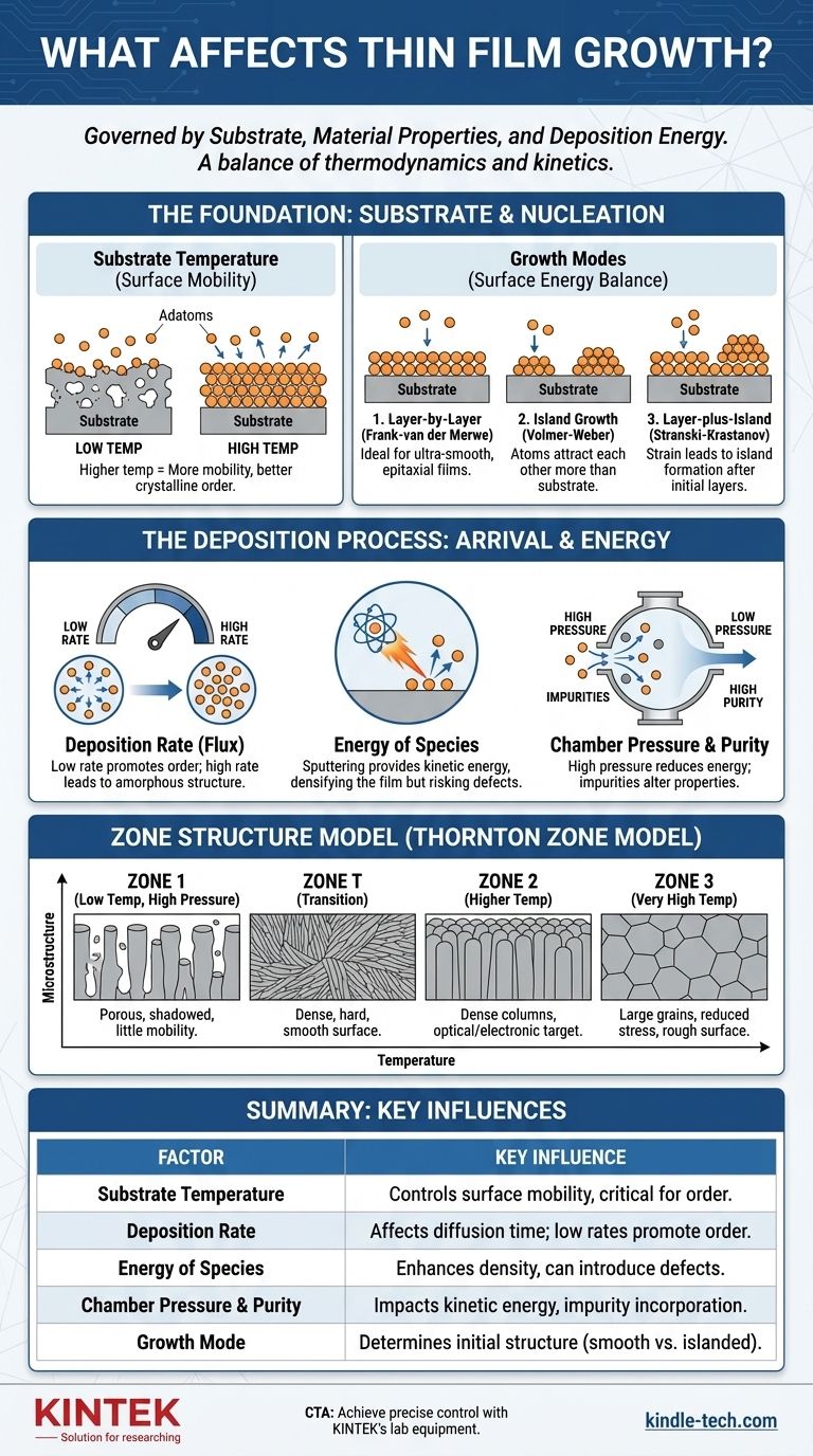
Substrate temperature is a direct control for surface mobility. A higher temperature provides more thermal energy to the arriving adatoms, allowing them to move across the surface for longer distances before locking into place. This mobility is crucial for forming ordered, crystalline structures.
The Balance of Surface Energies
How atoms first cluster on the surface is determined by the balance between the film material's surface energy, the substrate's surface energy, and the interface energy between them. This balance dictates one of three primary growth modes.
Frank-van der Merwe (Layer-by-Layer)
This mode occurs when the adatoms are more strongly attracted to the substrate than to each other. The material "wets" the surface, forming a complete, two-dimensional monolayer before a second layer begins to form. This is the ideal for creating ultra-smooth, epitaxial films.
Volmer-Weber (Island Growth)
Conversely, this mode occurs when adatoms are more strongly attracted to each other than to the substrate. The arriving atoms quickly cluster together, forming distinct three-dimensional islands that eventually grow and merge to form a continuous film.
Stranski-Krastanov (Layer-plus-Island)
This is a hybrid mode that starts with layer-by-layer growth. After one or more complete monolayers are formed, accumulated strain within the film makes it energetically favorable for subsequent growth to switch to island formation.
The Deposition Process: Controlling Arrival and Energy
Beyond the substrate, the method used to transport material—such as sputtering, evaporation, or chemical vapor deposition—provides the primary levers for controlling the film's final structure.
Deposition Rate
The deposition rate (or flux) determines how quickly atoms arrive at the surface. A low deposition rate gives adatoms more time to diffuse and find low-energy sites, promoting crystalline order. A very high rate can "bury" atoms before they have time to move, often resulting in an amorphous or poorly-ordered structure.
Energy of Deposited Species
Techniques like sputtering don't just deliver atoms; they deliver them with significant kinetic energy. This energy can enhance surface mobility, dislodge weakly-bonded atoms, and densify the film as it grows. However, excessive energy can also introduce defects and compressive stress.
Chamber Pressure and Purity
The pressure of the deposition chamber affects the mean free path of the atoms traveling from the source to the substrate. Higher background gas pressure can lead to collisions that reduce the atoms' kinetic energy upon arrival. Furthermore, impurities in the chamber (like water or oxygen) can be incorporated into the film, dramatically altering its properties.
Understanding the Trade-offs: The Zone Structure Model
A powerful framework for understanding the interplay of these factors is the Thornton Zone Model (TSZ Model). It maps the resulting film microstructure to two key parameters: substrate temperature and sputtering gas pressure.
Zone 1: Porous Structures
At low temperatures, adatoms have very little surface mobility and stick where they land. This creates a porous, columnar structure with significant voids, as high points on the growing film shadow the valleys from the incoming flux.
Zone T: Dense, Fibrous Grains
As temperature increases, surface diffusion begins to overcome the shadowing effect. This "T" or transition zone is characterized by a dense structure of fibrous grains with tightly packed boundaries, often yielding a hard film with a smooth surface.
Zone 2: Densely Packed Columns
At higher temperatures, surface diffusion becomes significant. The film grows as densely packed columnar grains that extend through the thickness of the film. This is often the target for many optical and electronic applications.
Zone 3: Large, Equiaxed Grains
At very high temperatures (typically over half the melting point of the film material), both surface and bulk diffusion are active. The initial columnar grains recrystallize into larger, three-dimensional equiaxed grains, which can reduce stress but also increase surface roughness.
Making the Right Choice for Your Goal
Controlling thin film growth is about purposefully manipulating these factors to achieve a specific microstructure and the desired material properties.
- If your primary focus is a highly-ordered, epitaxial film: Use a high substrate temperature, a very low deposition rate, and an ultra-high vacuum environment on a lattice-matched substrate.
- If your primary focus is a hard, dense coating: Target the Zone T or low-Zone 2 temperature range while using a process like sputtering to provide some kinetic energy for densification.
- If your primary focus is high-rate deposition for a simple barrier: A lower temperature, higher-rate process may be sufficient, even if it results in a less-ordered Zone 1 structure.
Ultimately, mastering thin film growth is about understanding and controlling the energy landscape on which your film is built.

Summary Table:
| Factor | Key Influence on Film Growth |
|---|---|
| Substrate Temperature | Controls surface mobility of atoms, critical for crystalline order. |
| Deposition Rate | Affects atom diffusion time; low rates promote ordered structures. |
| Energy of Deposited Species | Enhances density but can introduce defects; key in sputtering. |
| Chamber Pressure & Purity | Impacts kinetic energy and incorporation of impurities. |
| Growth Mode (e.g., Layer-by-Layer) | Determines initial film structure (smooth vs. islanded). |
Ready to achieve precise control over your thin film deposition process? The right lab equipment is fundamental to manipulating these critical growth factors. At KINTEK, we specialize in providing high-performance sputtering systems, evaporation sources, and CVD reactors designed to deliver the precise temperature control, deposition rates, and energy conditions your research demands. Let our experts help you select the ideal solution to grow high-quality, uniform thin films for your specific application—from epitaxial layers for electronics to hard, dense coatings.
Contact our thin film specialists today to discuss your project requirements and optimize your deposition process.
Visual Guide
