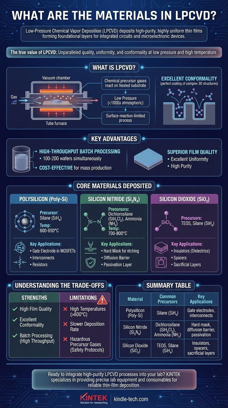
In short, Low-Pressure Chemical Vapor Deposition (LPCVD) is primarily used to deposit high-purity, highly uniform thin films of polysilicon, silicon nitride (Si₃N₄), and **silicon dioxide (SiO₂) **. These materials form the foundational layers for manufacturing integrated circuits and other microelectronic devices.
The true value of LPCVD isn't just the materials it can deposit, but the unparalleled quality it achieves. By operating at low pressure and high temperatures, the process produces films with excellent uniformity and an ability to perfectly coat complex 3D structures, making it indispensable for modern device fabrication.
What is LPCVD and Why Is It Used?
LPCVD is a process where chemical precursor gases react on the surface of a heated substrate inside a vacuum chamber. This reaction forms a solid thin film of the desired material. The "low-pressure" aspect is the defining characteristic that drives its primary advantages.
The Critical Role of Low Pressure
Operating at pressures 100 to 1000 times lower than atmospheric pressure dramatically increases the mean free path of the gas molecules. This means molecules travel further before colliding with each other.
This leads to a surface-reaction-limited process, where the deposition rate is governed by the chemical reaction on the substrate surface, not by how fast gas can get there. The direct result is excellent conformality—the ability to deposit a film of uniform thickness over complex, high-aspect-ratio trenches and steps.
The Batch Processing Advantage
LPCVD is typically performed in horizontal or vertical tube furnaces. Wafers can be stacked vertically with only a small gap between them, allowing for the processing of 100 to 200 wafers simultaneously.
This high-throughput, batch processing capability makes LPCVD an extremely cost-effective method for depositing the high-quality films required in mass production.
Core Materials Deposited by LPCVD
While many materials can theoretically be deposited, the process is optimized for a few key films that are critical to semiconductor manufacturing.
Polysilicon (Poly-Si)
Polysilicon is one of the most important materials in microelectronics. LPCVD is the standard method for depositing it using a precursor gas like silane (SiH₄) at temperatures around 600-650°C.
It is used primarily as the gate electrode in MOSFET transistors. It can also be heavily doped to make it conductive for use as interconnects or resistors.
Silicon Nitride (Si₃N₄)
Deposited using gases like dichlorosilane (SiH₂Cl₂) and ammonia (NH₃) at 700-800°C, LPCVD silicon nitride is a dense, robust material.
Its key applications include serving as a hard mask for etching, a diffusion barrier to prevent contaminants from reaching the active device, and a final passivation layer to protect the chip from moisture and damage.
Silicon Dioxide (SiO₂)
LPCVD is used to deposit several types of silicon dioxide. These are often referred to as "TEOS" films if they use tetraethylorthosilicate (TEOS) as a precursor, which is less hazardous than silane.
These oxide films are used as insulators (dielectrics) between conductive layers, as spacers to define device features, or as sacrificial layers that are later removed. The specific type, like Low-Temperature Oxide (LTO) or High-Temperature Oxide (HTO), is chosen based on the process temperature constraints.
Understanding the Trade-offs
LPCVD is a powerful tool, but it is not universally applicable. Its primary limitation is a direct consequence of its greatest strength.
The High-Temperature Limitation
The high temperatures required for LPCVD (typically >600°C) are its biggest drawback. This heat can damage or alter structures already fabricated on the wafer, such as metal interconnects (e.g., aluminum, which has a low melting point).
For this reason, LPCVD is almost exclusively used in the "Front-End-Of-Line" (FEOL) portion of chip manufacturing, before temperature-sensitive metals are deposited. For later steps requiring insulation, a lower-temperature process like Plasma-Enhanced CVD (PECVD) is used instead.
Film Quality vs. Deposition Rate
While LPCVD produces exceptionally high-quality films, its deposition rate is relatively slow compared to other methods like atmospheric pressure CVD (APCVD). The trade-off is clear: sacrificing speed for superior purity, uniformity, and conformality.
Precursor Gas Safety
The gases used in LPCVD, particularly silane, are often pyrophoric (ignite spontaneously in air) and highly toxic. This necessitates complex and expensive safety protocols and gas handling systems, adding to the operational overhead of the process.
Making the Right Choice for Your Goal
When selecting a deposition technique, your primary objective determines the best path forward.
- If your primary focus is ultimate film quality and conformality: LPCVD is the undisputed choice for materials like polysilicon and silicon nitride, especially for critical layers in FEOL processing.
- If your primary focus is depositing a film at low temperatures: You must use an alternative like Plasma-Enhanced CVD (PECVD), even if it means accepting lower film density and conformality.
- If your primary focus is high-speed, lower-quality deposition: A method like Atmospheric Pressure CVD (APCVD) might be more suitable for less critical, thick-film applications.
Ultimately, understanding the interplay between temperature, film properties, and device structure is the key to leveraging the power of LPCVD effectively.
Summary Table:
| Material | Common Precursors | Key Applications |
|---|---|---|
| Polysilicon (Poly-Si) | Silane (SiH₄) | Gate electrodes, interconnects |
| Silicon Nitride (Si₃N₄) | Dichlorosilane (SiH₂Cl₂), Ammonia (NH₃) | Hard mask, diffusion barrier, passivation |
| Silicon Dioxide (SiO₂) | TEOS, Silane (SiH₄) | Insulators, spacers, sacrificial layers |
Ready to integrate high-purity LPCVD processes into your lab? KINTEK specializes in providing the precise lab equipment and consumables you need for reliable thin-film deposition. Our expertise ensures you achieve the excellent uniformity and conformality critical for semiconductor and microdevice fabrication. Contact our experts today to discuss how we can support your specific application and enhance your research and production capabilities.
Visual Guide
Related Products
- Inclined Rotary Plasma Enhanced Chemical Vapor Deposition PECVD Equipment Tube Furnace Machine
- Inclined Rotary Plasma Enhanced Chemical Vapor Deposition PECVD Equipment Tube Furnace Machine
- Chemical Vapor Deposition CVD Equipment System Chamber Slide PECVD Tube Furnace with Liquid Gasifier PECVD Machine
- Laboratory CVD Boron Doped Diamond Materials
- Microwave Plasma Chemical Vapor Deposition MPCVD Machine System Reactor for Lab and Diamond Growth
People Also Ask
- What is plasma enhanced chemical vapour deposition PECVD used for? Enable Low-Temp Thin Films for Electronics & Solar
- What is the core value of PECVD compared to CVD? Discover the Low-Temperature Advantage for Thin-Film Coating
- What is Plasma Enhanced Chemical Vapor Deposition (PECVD)? High-Quality Film Deposition at Low Temperatures
- How does plasma enhance CVD? Unlock Low-Temperature, High-Quality Film Deposition
- What is plasma enhanced chemical vapor deposition PECVD equipment? A Guide to Low-Temperature Thin Film Deposition


