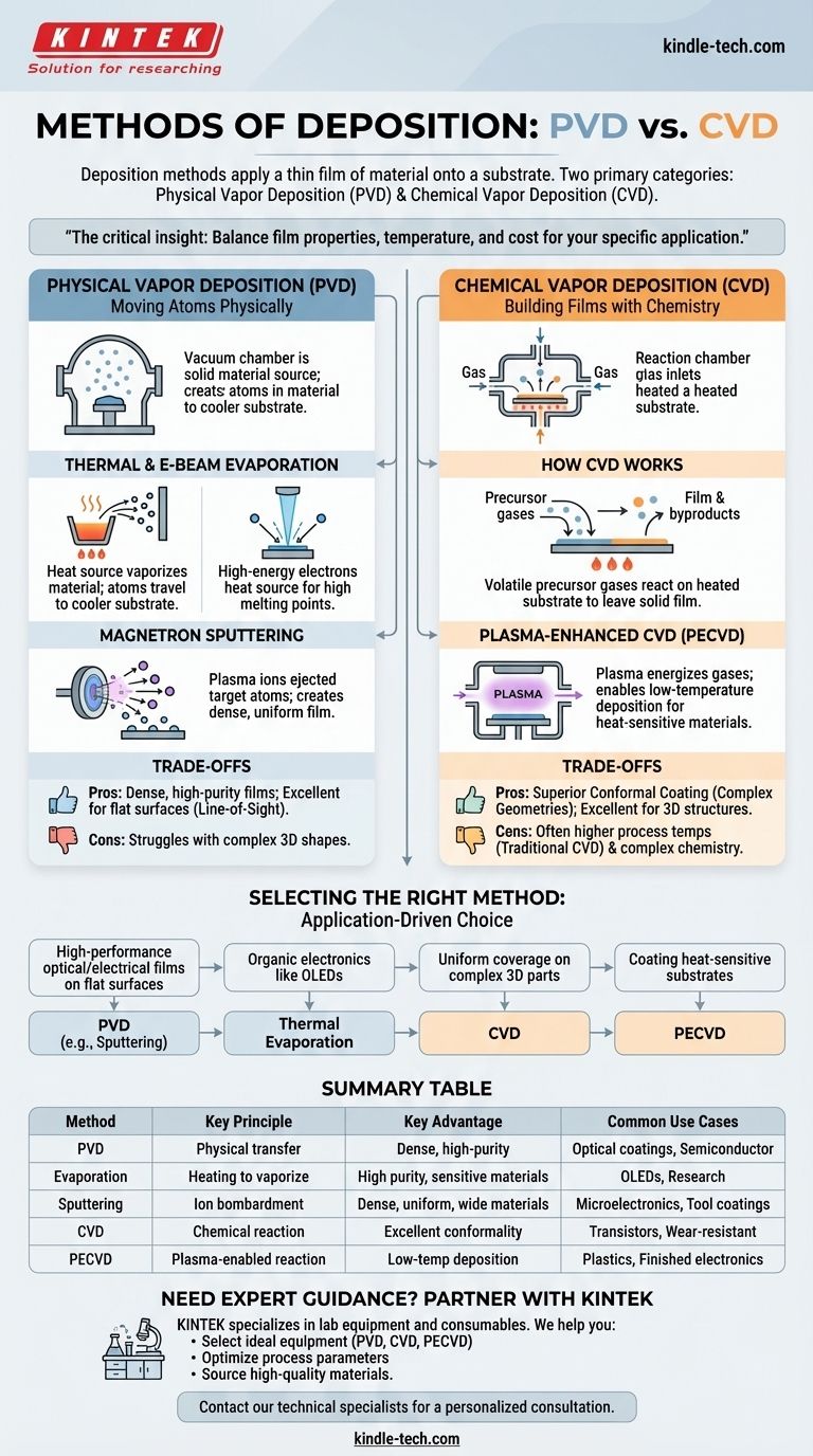
In short, deposition methods are techniques used to apply a thin film of material onto a surface, or substrate. These methods are fundamentally divided into two major categories: Physical Vapor Deposition (PVD), where a material is physically transferred to the substrate, and Chemical Vapor Deposition (CVD), where a film is grown on the substrate from chemical precursors.
The critical insight is not which deposition method is "best," but which technique provides the right balance of film properties, deposition temperature, and cost for a specific application—from making computer chips to coating sunglasses.
The Two Pillars of Deposition: PVD and CVD
To understand deposition, it's essential to recognize the two fundamentally different approaches. The choice between them dictates the equipment, process, and final characteristics of the thin film.
Physical Vapor Deposition (PVD): Moving Atoms Physically
PVD encompasses a family of methods where a solid or liquid source material is converted into a vapor and transported to the substrate for condensation. This is a line-of-sight process, much like spray painting, but on an atomic level.
The two most common PVD methods are evaporation and sputtering.
Thermal & E-Beam Evaporation
In thermal evaporation, a source material is heated in a high vacuum until its atoms evaporate and travel to the cooler substrate, where they condense to form a film.
Electron-beam (e-beam) evaporation is a more advanced version. It uses a high-energy beam of electrons to heat the source material, allowing for the deposition of materials with very high melting points.
Magnetron Sputtering
Sputtering can be thought of as atomic-scale sandblasting. High-energy ions from a plasma are accelerated into a "target" made of the desired coating material.
This collision ejects, or "sputters," atoms from the target, which then travel and deposit onto the substrate, creating a dense and uniform film.
Chemical Vapor Deposition (CVD): Building Films with Chemistry
CVD is fundamentally different from PVD. Instead of physically moving atoms, CVD uses chemical reactions to grow a film directly on the substrate's surface.
How CVD Works
In a CVD process, one or more volatile precursor gases are introduced into a reaction chamber. When these gases come into contact with the heated substrate, they react or decompose, leaving a solid thin film behind.
Plasma-Enhanced CVD (PECVD)
A key limitation of traditional CVD is the high temperature required to drive the chemical reactions. Plasma-Enhanced CVD (PECVD) solves this problem.
By using a plasma to energize the precursor gases, PECVD allows the necessary chemical reactions to occur at much lower temperatures, making it suitable for coating materials that cannot withstand high heat, such as plastics or completed electronic devices.
Understanding the Trade-offs
Choosing a deposition method always involves balancing competing factors. What makes one method ideal for one application can make it unsuitable for another.
PVD: Line-of-Sight and Dense Films
The primary advantage of PVD methods like sputtering is the ability to create extremely dense, pure, and high-quality films.
However, because it is a line-of-sight process, PVD struggles to uniformly coat complex, three-dimensional shapes with undercuts or hidden surfaces.
CVD: Superior Conformal Coating
CVD's main strength is its excellent conformality. Because the precursor gases can flow around and into complex geometries, CVD can deposit a highly uniform film over intricate 3D structures.
The main trade-off is often higher process temperatures (for traditional CVD) and more complex chemistry compared to PVD.
Selecting the Right Method for Your Application
Your final choice depends entirely on the requirements of your end product.
- If your primary focus is high-performance optical or electrical films on flat surfaces: PVD methods like magnetron sputtering are often the ideal choice for their density and purity.
- If your primary focus is creating organic electronics like OLEDs: Thermal evaporation is a well-established and effective technique for these sensitive materials.
- If your primary focus is uniform coverage on complex 3D parts: A CVD process is almost always the superior option due to its excellent conformality.
- If your primary focus is coating heat-sensitive substrates: PECVD is specifically designed for these applications, allowing for high-quality chemical deposition at lower temperatures.
Ultimately, understanding the fundamental physics and chemistry of each method is the key to selecting the right tool for the job.
Summary Table:
| Method | Key Principle | Key Advantage | Common Use Cases |
|---|---|---|---|
| PVD (Physical Vapor Deposition) | Physical transfer of material to substrate | Dense, high-purity films; good for flat surfaces | Optical coatings, semiconductor metallization |
| Evaporation | Heating source material to vaporize it | High purity; good for sensitive materials | OLEDs, research applications |
| Sputtering | Ejecting target atoms via ion bombardment | Dense, uniform films; wide material selection | Microelectronics, durable tool coatings |
| CVD (Chemical Vapor Deposition) | Chemical reaction on substrate surface | Excellent conformal coating on complex shapes | Semiconductor transistors, wear-resistant coatings |
| PECVD (Plasma-Enhanced CVD) | Uses plasma to enable lower temperature reactions | High-quality films on heat-sensitive materials | Coating plastics, finished electronics |
Need Expert Guidance on Your Deposition Process?
Choosing the right deposition method is critical to the success of your project. The wrong technique can lead to poor film quality, higher costs, and project delays.
KINTEK is your partner in precision. We specialize in lab equipment and consumables for all your deposition needs. Our experts can help you:
- Select the ideal equipment (PVD, CVD, or PECVD) for your specific material and substrate.
- Optimize your process parameters to achieve the desired film properties.
- Source high-quality targets, precursors, and consumables for reliable, repeatable results.
Don't leave your coating application to chance. Contact our technical specialists today for a personalized consultation and let us help you achieve superior thin-film results.
Visual Guide
Related Products
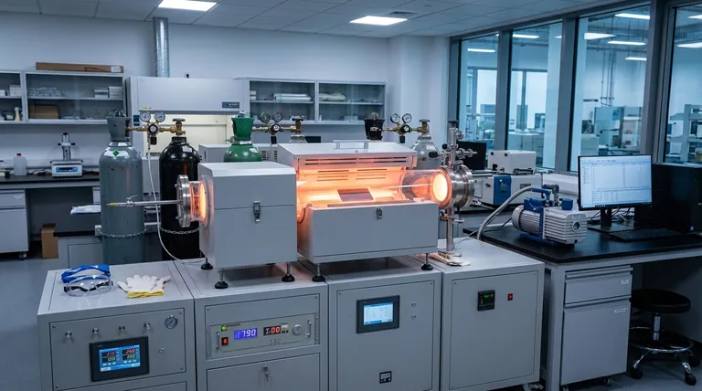
- Chemical Vapor Deposition CVD Equipment System Chamber Slide PECVD Tube Furnace with Liquid Gasifier PECVD Machine
- Customer Made Versatile CVD Tube Furnace Chemical Vapor Deposition Chamber System Equipment
- HFCVD Machine System Equipment for Drawing Die Nano-Diamond Coating
- Split Chamber CVD Tube Furnace with Vacuum Station Chemical Vapor Deposition System Equipment Machine
- Multi Heating Zones CVD Tube Furnace Machine Chemical Vapor Deposition Chamber System Equipment
People Also Ask
- How are carbon nanotubes grown? Master Scalable Production with Chemical Vapor Deposition
- How expensive is chemical vapor deposition? Understanding the True Cost of High-Performance Coating
- Why is Chemical Vapor Deposition (CVD) equipment uniquely suited for constructing hierarchical superhydrophobic structures?
- What are the advantages of chemical vapor deposition? Achieve Superior Thin Films for Your Lab
- What happens during deposition chemistry? Building Thin Films from Gaseous Precursors


