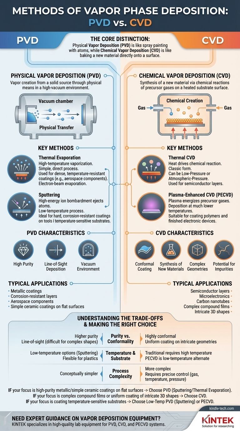
At its core, vapor deposition is divided into two fundamental families: Physical Vapor Deposition (PVD) and Chemical Vapor Deposition (CVD). PVD methods use physical processes like evaporation or sputtering to transfer a material from a source to a substrate. In contrast, CVD methods use chemical reactions from precursor gases to grow a new material directly on the substrate's surface.
The critical distinction isn't the equipment, but the underlying process: Physical Vapor Deposition (PVD) is like spray-painting with atoms, while Chemical Vapor Deposition (CVD) is like baking a new material directly onto a surface.
The Two Pillars of Vapor Deposition
Vapor phase deposition encompasses any process where a thin solid film is formed on a surface from a material in its gaseous or vapor state. Understanding the fundamental split between physical and chemical methods is the first step in selecting the right technique for a specific application.
Physical Vapor Deposition (PVD)
PVD processes involve the creation of a vapor from a solid source material through purely physical means, all conducted in a high-vacuum environment. The resulting film has the same basic chemical composition as the source material.
Chemical Vapor Deposition (CVD)
CVD processes involve introducing one or more volatile precursor gases into a reaction chamber. These gases decompose or react on a heated substrate, leaving behind a solid film of a new material. The film's composition is a result of this chemical reaction.
A Deeper Look at Physical Vapor Deposition (PVD)
The goal of PVD is to physically move atoms from a source target to a substrate. The two dominant methods achieve this in different ways.
Key Method: Thermal Evaporation
This is the most straightforward PVD technique. A source material is heated in a vacuum chamber until its atoms gain enough energy to vaporize. These gaseous atoms then travel through the vacuum and condense onto the cooler substrate, forming a film.
For example, electron-beam evaporation is used by aerospace companies to apply dense, temperature-resistant coatings to critical components.
Key Method: Sputtering
Sputtering does not rely on heat. Instead, a target of the source material is bombarded with high-energy ions (typically from an inert gas like argon). This energetic collision physically ejects or "sputters" atoms from the target, which then deposit onto the substrate.
This method is excellent for applying very hard, corrosion-resistant coatings to tools and other products used in harsh environments.
A Deeper Look at Chemical Vapor Deposition (CVD)
CVD is fundamentally a process of synthesis. You are not just moving a material; you are creating one on the surface of your substrate.
The Core Principle: A Surface Chemical Reaction
In all CVD processes, precursor gases flow over a substrate inside a reaction chamber. Energy is applied to the system, causing the gases to react or decompose on the hot surface, building up the desired film layer by layer.
Key Method: Thermal CVD
This is the classic form of CVD, where heat is the sole energy source driving the chemical reaction. Its effectiveness can be limited by either the speed of the surface reaction (Low-Pressure CVD) or the speed at which gases can reach the surface (Atmospheric-Pressure CVD).
Key Method: Plasma-Enhanced CVD (PECVD)
Instead of relying only on high temperatures, PECVD uses a plasma to energize the precursor gases. This allows deposition to occur at much lower temperatures, making it suitable for substrates that cannot withstand intense heat.
Common CVD Applications
CVD is a workhorse in the electronics industry for creating the precise semiconducting and insulating layers in microchips. It is also frequently used to grow advanced materials like carbon nanotubes and GaN nanowires.
Understanding the Trade-offs
Choosing between PVD and CVD requires understanding their inherent advantages and limitations.
Purity vs. Conformality
PVD generally produces higher-purity films because you are simply transferring a source material. However, it is a "line-of-sight" process, making it difficult to evenly coat complex, three-dimensional shapes.
CVD excels at creating highly conformal coatings that uniformly cover intricate geometries. The trade-off is the potential for impurities from chemical byproducts.
Temperature and Substrate
Traditional thermal CVD requires very high temperatures, which limits the types of materials that can be used as a substrate.
PVD methods like sputtering and specialized CVD methods like PECVD can operate at much lower temperatures, offering greater flexibility for coating temperature-sensitive materials like plastics.
Process Complexity
PVD is often a conceptually simpler and more direct process. CVD can be more complex, requiring precise control over gas flows, temperature, and pressure, and often demands a higher level of operator skill.
Making the Right Choice for Your Goal
Your application's specific requirements will dictate the best deposition method.
- If your primary focus is high-purity metallic or simple ceramic coatings on a relatively flat surface: PVD, particularly sputtering or thermal evaporation, is often the most direct and effective choice.
- If your primary focus is creating a complex compound film (like silicon nitride) or coating intricate 3D shapes uniformly: CVD is almost certainly the superior technology.
- If your primary focus is coating a temperature-sensitive substrate (like a polymer or a finished electronic device): Your best options are low-temperature PVD methods like sputtering or a specialized technique like Plasma-Enhanced CVD (PECVD).
Ultimately, understanding whether your goal requires a physical transfer or a chemical creation is the key to navigating the world of vapor deposition.
Summary Table:
| Method | Process Type | Key Characteristics | Typical Applications |
|---|---|---|---|
| Physical Vapor Deposition (PVD) | Physical transfer | Line-of-sight deposition, high purity, vacuum environment | Metallic coatings, corrosion-resistant layers, aerospace components |
| Chemical Vapor Deposition (CVD) | Chemical reaction | Conformal coating, complex geometries, synthesis of new materials | Semiconductor layers, microelectronics, carbon nanotubes |
| Thermal Evaporation | PVD | Simple process, high-temperature vaporization | Dense, temperature-resistant coatings |
| Sputtering | PVD | Low-temperature process, non-thermal atom ejection | Hard coatings, tools, temperature-sensitive substrates |
| Plasma-Enhanced CVD (PECVD) | CVD | Low-temperature operation, plasma-assisted reaction | Coating polymers, finished electronic devices |
Need Expert Guidance on Vapor Deposition Equipment?
Choosing between PVD and CVD methods is critical for your thin film application success. KINTEK specializes in high-quality lab equipment and consumables for all your vapor deposition needs.
We provide:
- Advanced PVD systems for high-purity metallic coatings
- Precision CVD reactors for complex material synthesis
- Plasma-Enhanced CVD equipment for temperature-sensitive substrates
- Complete solutions for semiconductor, aerospace, and research applications
Let our experts help you select the perfect deposition method for your specific requirements.
Contact KINTEK today to discuss your project and discover how our vapor deposition solutions can enhance your research and production outcomes!
Visual Guide
Related Products
- Chemical Vapor Deposition CVD Equipment System Chamber Slide PECVD Tube Furnace with Liquid Gasifier PECVD Machine
- RF PECVD System Radio Frequency Plasma-Enhanced Chemical Vapor Deposition RF PECVD
- Microwave Plasma Chemical Vapor Deposition MPCVD Machine System Reactor for Lab and Diamond Growth
- 915MHz MPCVD Diamond Machine Microwave Plasma Chemical Vapor Deposition System Reactor
- Customer Made Versatile CVD Tube Furnace Chemical Vapor Deposition Chamber System Equipment
People Also Ask
- What is plasma enhanced chemical vapor deposition PECVD equipment? A Guide to Low-Temperature Thin Film Deposition
- What happens during deposition chemistry? Building Thin Films from Gaseous Precursors
- How expensive is chemical vapor deposition? Understanding the True Cost of High-Performance Coating
- Why is Chemical Vapor Deposition (CVD) equipment uniquely suited for constructing hierarchical superhydrophobic structures?
- What types of substrates are used in CVD to facilitate graphene films? Optimize Graphene Growth with the Right Catalyst


