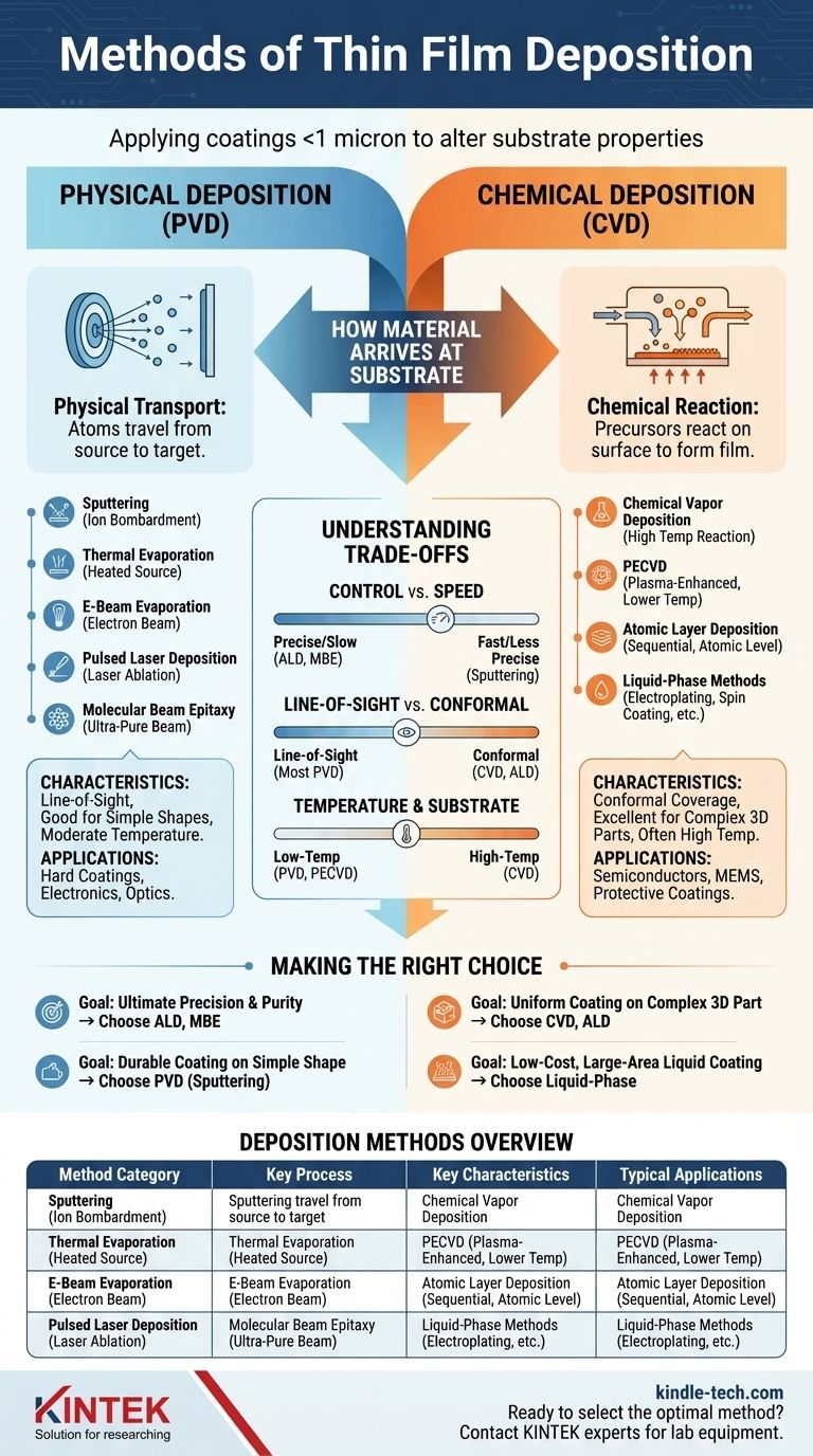
At its core, thin film deposition involves applying a material coating, often less than a micron thick, onto a substrate to alter its properties. The methods for achieving this are broadly divided into two fundamental categories: Physical Deposition and Chemical Deposition, each using a distinct approach to build the film layer by layer.
The critical distinction lies in how the material arrives at the substrate. Physical methods physically transport atoms from a source to the target, while chemical methods use precursor materials that undergo a chemical reaction on the substrate's surface to form the film.

The Two Pillars of Deposition: Physical vs. Chemical
Understanding the fundamental mechanism behind each category is key to selecting the right process for a specific application, whether it's for semiconductors, optics, or protective coatings.
Physical Vapor Deposition (PVD): Transporting Material
In PVD processes, the coating material starts as a solid or liquid in a vacuum chamber. Energy is applied to create a vapor of atoms or molecules that then travel through the vacuum and condense onto the substrate.
The primary PVD methods include:
- Sputtering: A target of the coating material is bombarded with high-energy ions, which knock atoms loose that then deposit onto the substrate.
- Thermal Evaporation: The source material is heated in a vacuum until it evaporates, with the vapor condensing on the cooler substrate.
- Electron Beam Evaporation: A high-energy electron beam is aimed at the source material, causing localized boiling and evaporation for deposition.
- Pulsed Laser Deposition (PLD): A high-power laser ablates the surface of a target, creating a plasma plume that deposits onto the substrate.
- Molecular Beam Epitaxy (MBE): This high-precision technique evaporates elemental sources to create an ultra-pure beam of atoms or molecules that form a highly ordered, crystalline film on the substrate.
Chemical Deposition: Building with Precursors
Chemical deposition methods introduce one or more volatile precursor materials, typically gases or liquids, into a reaction chamber. These precursors react or decompose on the substrate's surface to create the desired film.
The primary chemical methods include:
- Chemical Vapor Deposition (CVD): Precursor gases are introduced into a chamber where they react at high temperatures on the substrate surface to form a non-volatile solid film.
- Plasma-Enhanced CVD (PECVD): A variation of CVD that uses a plasma to energize the precursor gases, allowing the reaction to occur at much lower temperatures.
- Atomic Layer Deposition (ALD): A highly controlled process that uses sequential, self-limiting chemical reactions to build a film one single atomic layer at a time.
- Liquid-Phase Methods: Simpler methods for certain materials include electroplating (using an electric current to reduce dissolved metal cations), sol-gel, dip coating, and spin coating (all of which apply a liquid precursor that is then solidified).
Understanding the Trade-offs
No single method is universally superior. The choice is always a matter of balancing competing requirements for the final product, such as performance, cost, and material compatibility.
Control vs. Speed
Processes like Atomic Layer Deposition (ALD) and Molecular Beam Epitaxy (MBE) offer unparalleled, atomic-level control over film thickness and structure. This precision comes at the cost of being very slow and complex.
In contrast, methods like sputtering or thermal evaporation are generally much faster and more economical for applying thicker coatings where atomic precision is not the primary concern.
Line-of-Sight vs. Conformal Coverage
Most PVD techniques are "line-of-sight," meaning the coating material travels in a straight line from the source to the substrate. This makes it very difficult to uniformly coat complex, three-dimensional shapes with undercuts or internal surfaces.
Chemical methods, especially CVD and ALD, excel at creating conformal coatings. Because the precursor gases can flow around complex geometries, they can deposit a highly uniform film over every exposed surface of an intricate part.
Temperature and Substrate Sensitivity
Traditional CVD often requires very high temperatures to drive the necessary chemical reactions. This can easily damage sensitive substrates like polymers or certain semiconductor devices.
PVD methods and low-temperature variants like PECVD are often better suited for heat-sensitive materials, as the deposition can occur much closer to room temperature.
Making the Right Choice for Your Goal
Your final application dictates the ideal deposition method. By focusing on your primary objective, you can narrow down the choices to the most suitable category.
- If your primary focus is ultimate precision and film purity: Methods like Atomic Layer Deposition (ALD) and Molecular Beam Epitaxy (MBE) are the industry standards for their atomic-level control.
- If your primary focus is a durable, functional coating on a simple shape: Physical Vapor Deposition (PVD) techniques like sputtering are robust, versatile, and widely used for everything from hard coatings on tools to metallic layers in electronics.
- If your primary focus is a perfectly uniform coating on a complex 3D part: Chemical Vapor Deposition (CVD) and its variants provide superior conformal coverage that PVD methods cannot match.
- If your primary focus is a low-cost, large-area coating from a liquid precursor: Solution-based processes like spin coating or dip coating are efficient for materials like polymers or sol-gels.
Ultimately, selecting the correct technique begins with understanding whether your goal is best served by physically moving a material or by chemically building it in place.
Summary Table:
| Method Category | Key Process | Key Characteristics | Typical Applications |
|---|---|---|---|
| Physical Vapor Deposition (PVD) | Sputtering, Evaporation | Line-of-sight, good for simple shapes, moderate temperature | Hard coatings, electronics, optics |
| Chemical Vapor Deposition (CVD) | CVD, PECVD, ALD | Conformal coverage, excellent for complex 3D parts, often high temperature | Semiconductors, MEMS, protective coatings |
| Liquid-Phase Methods | Spin Coating, Electroplating | Low-cost, large-area coverage, simpler equipment | Photoresists, sol-gel films, decorative coatings |
Ready to select the optimal thin film deposition method for your project? The experts at KINTEK are here to help. We specialize in providing high-quality lab equipment and consumables for all your deposition needs, from robust PVD sputtering systems to precise ALD reactors. Let us help you achieve the perfect coating for your application in semiconductors, optics, or protective layers. Contact our team today to discuss your specific requirements and discover the KINTEK advantage!
Visual Guide
Related Products
- Aluminized Ceramic Evaporation Boat for Thin Film Deposition
- Tungsten Evaporation Boat for Thin Film Deposition
- Electron Beam Evaporation Coating Oxygen-Free Copper Crucible and Evaporation Boat
- Molybdenum Tungsten Tantalum Evaporation Boat for High Temperature Applications
- Vacuum Hot Press Furnace Machine for Lamination and Heating
People Also Ask
- Why is an alumina boat and Ti3AlC2 powder bed necessary for Ti2AlC sintering? Protect MAX Phase Purity
- What are thin films deposited by evaporation? A Guide to High-Purity Coating
- What is the widely used boat made of in thermal evaporation? Choosing the Right Material for High-Purity Deposition
- What are the alternatives to sputtering? Choose the Right Thin Film Deposition Method
- Why is an alumina boat selected for catalyst precursors? Ensure Sample Purity at 1000 °C


