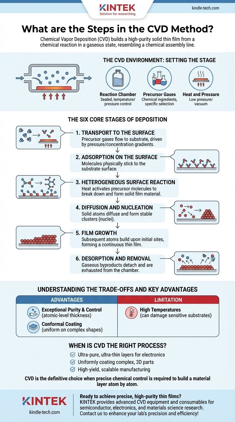
At its core, Chemical Vapor Deposition (CVD) is a sophisticated process that builds a solid, high-purity thin film on a surface from a chemical reaction in a gaseous state. The process is defined by a sequence of six fundamental steps: transport of reactant gases to the substrate, their adsorption onto the surface, chemical reactions to form the film, and the subsequent removal of gaseous byproducts.
The essential concept of CVD is a chemical assembly line. Gaseous precursor molecules are delivered to a heated surface, where they react and assemble into a solid film, while the leftover chemical waste is systematically exhausted.
The CVD Environment: Setting the Stage
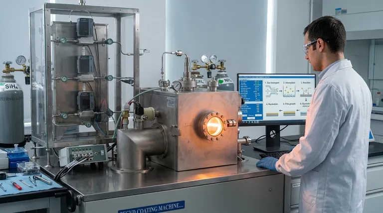
Before the deposition process can begin, the target object, known as the substrate, must be placed inside a controlled reaction chamber.
The Reaction Chamber
This is a sealed vessel where the entire process takes place. It allows for precise control over temperature, pressure, and the chemical environment.
The Precursor Gases
These are the chemical ingredients for the film. They are selected specifically to react under certain conditions to produce the desired solid material.
Heat and Pressure
The substrate is typically heated to a specific temperature that provides the energy needed to drive the chemical reaction. The chamber is often kept at a low pressure or in a vacuum to control the purity and movement of the gases.
The Six Core Stages of Deposition
The creation of a thin film via CVD is not a single event but a carefully orchestrated sequence of physical and chemical steps occurring at the microscopic level.
1. Transport to the Surface
First, the precursor gases are introduced into the reaction chamber. They flow towards the heated substrate, a process driven by pressure and concentration gradients.
2. Adsorption on the Surface
Once the precursor gas molecules reach the substrate, they physically stick to its surface. This process is called adsorption.
3. Heterogeneous Surface Reaction
This is the critical chemical step. The heat from the substrate provides the activation energy for the adsorbed precursor molecules to react, breaking down and forming new, stable solid molecules that will constitute the film.
4. Diffusion and Nucleation
The newly formed solid atoms are not static. They possess enough energy to diffuse or move across the surface until they find a stable, low-energy site to bond to. The initial formation of these stable clusters is called nucleation.
5. Film Growth
Following nucleation, subsequent atoms arriving on the surface build upon these initial sites. The film grows layer by layer, eventually forming a continuous, solid thin film of the desired thickness.
6. Desorption and Removal
The chemical reactions that form the solid film also create gaseous byproducts. These waste products detach (desorb) from the surface and are transported away from the substrate, eventually being exhausted from the chamber.
Understanding the Trade-offs and Key Advantages
CVD is a highly versatile and powerful technique, but its strengths come with specific considerations.
Advantage: Exceptional Purity and Control
Because the process starts with highly pure gases and occurs in a controlled environment, CVD can produce films of exceptional purity. It also allows for atomic-level control over thickness, making it essential for creating the ultra-thin layers required in electrical circuits and semiconductors.
Advantage: Conformal Coating
CVD is a non-line-of-sight process. The gas precursors surround the substrate, allowing the film to form uniformly on all surfaces, even on components with complex, three-dimensional shapes.
Limitation: High Temperatures
The need for high temperatures to drive the chemical reactions can be a significant drawback. These temperatures can damage or alter certain sensitive substrates, such as some polymers or pre-processed electronic components.
When is CVD the Right Process?
Choosing a deposition method depends entirely on the material requirements and the application's end goal.
- If your primary focus is creating ultra-pure, ultra-thin layers for electronics: CVD offers unparalleled control over film thickness, purity, and composition, which is critical for semiconductor manufacturing.
- If your primary focus is uniformly coating complex, three-dimensional parts: CVD's non-line-of-sight nature ensures a consistent and even film on all surfaces, which is difficult to achieve with other methods.
- If your primary focus is high-yield, scalable manufacturing: CVD processes are well-understood and can be effectively scaled up for the high-volume production of high-quality films.
Ultimately, Chemical Vapor Deposition is the definitive choice when precise chemical control is required to build a material layer atom by atom.
Summary Table:
| Step | Description | Key Action |
|---|---|---|
| 1. Transport | Precursor gases flow to substrate | Gas introduction & flow |
| 2. Adsorption | Molecules stick to substrate surface | Physical adhesion |
| 3. Surface Reaction | Chemical breakdown forms solid film | Chemical transformation |
| 4. Nucleation | Atoms form stable clusters on surface | Initial film formation |
| 5. Film Growth | Continuous layer-by-layer buildup | Thickness development |
| 6. Byproduct Removal | Waste gases detach and exhaust | Chamber cleaning |
Ready to achieve precise, high-purity thin films in your lab? KINTEK specializes in providing advanced CVD equipment and consumables tailored for semiconductor manufacturing, electronics, and materials science research. Our solutions deliver exceptional purity, conformal coating on complex shapes, and scalable production capabilities. Contact our experts today to discuss how our CVD technology can enhance your laboratory's precision and efficiency!
Visual Guide
Related Products
- Chemical Vapor Deposition CVD Equipment System Chamber Slide PECVD Tube Furnace with Liquid Gasifier PECVD Machine
- Customer Made Versatile CVD Tube Furnace Chemical Vapor Deposition Chamber System Equipment
- Microwave Plasma Chemical Vapor Deposition MPCVD Machine System Reactor for Lab and Diamond Growth
- 915MHz MPCVD Diamond Machine Microwave Plasma Chemical Vapor Deposition System Reactor
- Custom CVD Diamond Coating for Lab Applications
People Also Ask
- How are carbon nanotubes grown? Master Scalable Production with Chemical Vapor Deposition
- What types of substrates are used in CVD to facilitate graphene films? Optimize Graphene Growth with the Right Catalyst
- How expensive is chemical vapor deposition? Understanding the True Cost of High-Performance Coating
- What happens during deposition chemistry? Building Thin Films from Gaseous Precursors
- What is plasma enhanced chemical vapor deposition PECVD equipment? A Guide to Low-Temperature Thin Film Deposition


