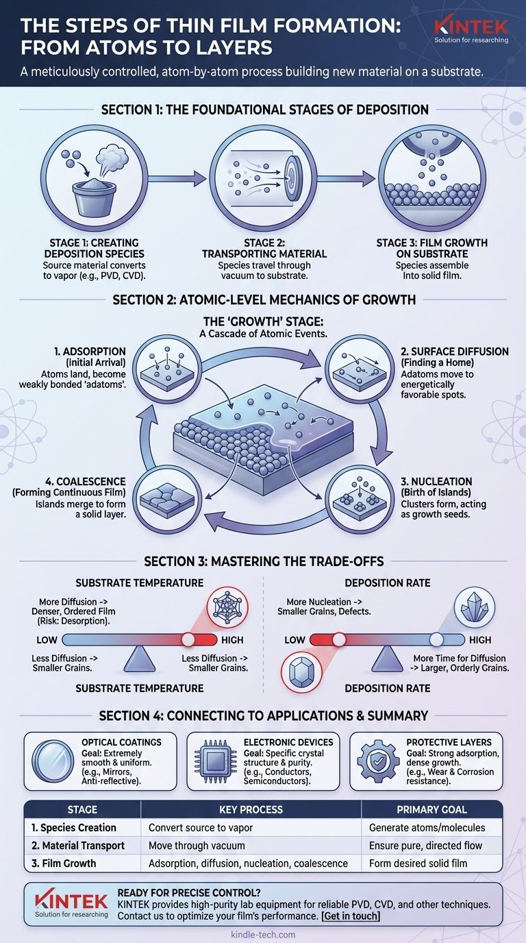
At its core, the formation of a thin film is a meticulously controlled process that builds a new material layer, atom by atom, on a substrate. The entire process can be broken down into three primary stages: the creation of atomic or molecular species from a source material, the transport of these species to a substrate, and finally, their controlled growth into a solid film on the substrate's surface.
Thin film formation is not simply a coating process; it is a sequence of atomic-level events. The final properties of the film are dictated by the interplay between atoms arriving at a surface (adsorption), moving across it (diffusion), and assembling into a stable structure (nucleation).
The Foundational Stages of Deposition
Every thin film deposition process, whether physical or chemical, follows a fundamental sequence to move material from a source to a substrate. This occurs within a highly controlled environment, typically a vacuum chamber, to ensure purity and precision.
Stage 1: Creating the Deposition Species
The first step is to generate the atoms or molecules that will form the film. This involves converting a solid or liquid source material into a vapor phase. The method used to do this is a primary differentiator between deposition techniques like Physical Vapor Deposition (PVD) or Chemical Vapor Deposition (CVD).
Stage 2: Transporting Material to the Substrate
Once the species are created, they must travel from the source to the target substrate. This journey happens through the vacuum chamber. The path and energy of these particles are critical variables that influence the quality and characteristics of the final film.
Stage 3: Film Growth on the Substrate Surface
This is the final and most complex stage, where the transported species arrive at the substrate and assemble into a solid, continuous film. This growth is not instantaneous but rather a cascade of distinct physical events at the atomic level.
The Atomic-Level Mechanics of Film Growth
The "growth" stage is where the film's ultimate structure and properties are truly defined. It consists of several competing physical phenomena happening simultaneously on the substrate surface.
Adsorption: The Initial Arrival
Atoms, ions, or molecules from the vapor phase first land on the substrate. This initial attachment is called adsorption. These newly arrived particles, often called "adatoms," are not yet part of a stable film and are often weakly bonded to the surface.
Surface Diffusion: Finding a Home
Adsorbed atoms are not static. Possessing thermal energy, they move and skate across the substrate's surface in a process known as surface diffusion. This movement allows them to find more energetically favorable locations, such as a surface defect or another adatom.
Nucleation: The Birth of Islands
As adatoms diffuse across the surface, they collide and bond with each other, forming small, stable clusters. This process is called nucleation. These clusters act as seeds, or nuclei, that attract other diffusing adatoms, causing them to grow into larger structures often referred to as "islands."
Coalescence and Growth: Forming a Continuous Film
As deposition continues, these islands grow larger and eventually merge, or coalesce. This process continues until the gaps between islands are filled, ultimately forming a continuous, solid thin film covering the entire substrate surface. The way in which these islands merge determines much of the film's final grain structure and surface roughness.
Understanding the Trade-offs
Controlling the atomic-level mechanics of growth is the key to engineering a film with specific properties. The balance between these phenomena is delicate and presents critical trade-offs.
The Impact of Substrate Temperature
A higher substrate temperature increases the energy of adatoms, promoting more surface diffusion. This allows atoms to find ideal crystalline positions, often resulting in a denser, more ordered film. However, too much energy can also increase desorption, where atoms detach from the surface and return to the vapor, slowing the growth rate.
The Role of Deposition Rate
A high deposition rate means more atoms are arriving on the surface per second. This increases the chance of nucleation because adatoms are more likely to find each other before they can diffuse very far. This can lead to a film with smaller grains and potentially more defects. A lower rate gives atoms more time to diffuse, often resulting in larger, more orderly crystal grains.
Connecting the Process to the Final Application
The choice of deposition parameters is always driven by the intended use of the thin film. By controlling the steps of formation, you can tailor the film's properties to meet specific performance goals.
- If your primary focus is optical coatings (e.g., mirrors, anti-reflective layers): You must control the growth to produce an extremely smooth and uniform film, as surface roughness can scatter light and degrade performance.
- If your primary focus is electronic devices (e.g., integrated circuits): The process must be precisely controlled to achieve a specific crystal structure and purity, which directly determines the film's electrical properties as a conductor, semiconductor, or insulator.
- If your primary focus is protective coatings (e.g., for tools or parts): The goal is to promote strong adsorption and dense growth (often through ion bombardment), creating a hard, well-adhered film that resists wear and corrosion.
Ultimately, mastering thin film formation means mastering the control of atomic-scale events to engineer desired macroscopic properties.
Summary Table:
| Stage | Key Process | Primary Goal |
|---|---|---|
| 1. Species Creation | Convert source material to vapor | Generate atoms/molecules for deposition |
| 2. Material Transport | Move species through vacuum to substrate | Ensure pure, directed particle flow |
| 3. Film Growth | Adsorption, diffusion, nucleation, coalescence | Form continuous solid film with desired properties |
Ready to achieve precise control over your thin film deposition process? The quality of your optical coatings, electronic devices, or protective layers depends on mastering these atomic-level steps. KINTEK specializes in providing the high-purity lab equipment and consumables needed for reliable PVD, CVD, and other deposition techniques. Our experts can help you select the right tools to optimize adsorption, diffusion, and nucleation for your specific application. Contact us today to discuss your project and enhance your film's performance. Get in touch with our specialists
Visual Guide