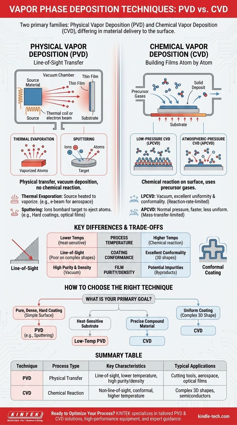
In short, vapor phase deposition techniques are categorized into two primary families: Physical Vapor Deposition (PVD) and Chemical Vapor Deposition (CVD). The core difference lies in how the material arrives at the surface. PVD physically transfers a solid material into a vapor that condenses onto the substrate, while CVD uses precursor gases that chemically react on the substrate's surface to form an entirely new solid film.
The fundamental choice between PVD and CVD is not about which technique is superior, but which process aligns with the specific requirements of the material and the part being coated. PVD is a line-of-sight physical transfer process, while CVD is a chemical reaction process that excels at coating complex surfaces uniformly.
Physical Vapor Deposition (PVD): A Line-of-Sight Transfer
Physical Vapor Deposition encompasses a set of vacuum deposition methods where a material is transformed into a vapor, transported across a vacuum chamber, and condensed onto a substrate as a thin film. This is a purely physical process with no intended chemical reactions.
Thermal Evaporation
In thermal evaporation, a source material is heated in a high vacuum until it vaporizes. These vaporized atoms then travel in a straight line until they strike the substrate, where they cool and condense to form a solid film.
A common variant is e-beam evaporation, which uses a high-energy electron beam to heat the source. This technique is often used by aerospace companies to apply dense, temperature-resistant coatings to critical components.
Sputtering
Sputtering involves bombarding a solid source material, known as a "target," with high-energy ions from a plasma. This collision physically ejects or "sputters" atoms from the target, which then travel and deposit onto the substrate.
This method is highly valued for creating hard, dense, and corrosion-resistant coatings for cutting tools and industrial components, as well as applying optical films for solar panels and semiconductors.
Chemical Vapor Deposition (CVD): Building Films Atom by Atom
Chemical Vapor Deposition is a process where a substrate is exposed to one or more volatile precursor gases. These gases react or decompose on the substrate's surface in a controlled environment, creating the desired solid deposit.
Low-Pressure CVD (LPCVD)
As the name implies, this process occurs in a vacuum or low-pressure environment. Under these conditions, the film's growth rate is limited by the speed of the chemical reaction on the surface itself.
This reaction-rate-limited nature allows the precursor gases to cover the entire surface before reacting, resulting in films with excellent thickness uniformity and the ability to conformally coat very complex shapes.
Atmospheric-Pressure CVD (APCVD)
This technique operates at normal atmospheric pressure, which simplifies equipment design. However, the reaction rate is mass-transfer-limited, meaning the film's growth is determined by how quickly the precursor gases can travel through the boundary layer to reach the substrate.
APCVD is generally a faster deposition process than LPCVD but often produces films that are less uniform, making it suitable for applications where perfect conformality is not the primary concern.
Understanding the Key Differences and Trade-offs
Choosing the correct technique requires understanding the fundamental trade-offs between these two families of deposition.
Process Temperature
CVD typically requires the substrate to be heated to high temperatures to provide the necessary energy to drive the chemical reactions. PVD can often be performed at much lower substrate temperatures, which is critical for heat-sensitive materials.
Coating Conformance
CVD is the superior choice for coating complex, non-flat surfaces. Because the process is driven by gases, it can uniformly coat intricate 3D geometries. PVD is a line-of-sight technique, making it very difficult to coat shadowed areas or undercuts without complex part rotation.
Film Purity and Density
PVD processes, especially sputtering, generally produce films with very high purity and density. This is because you are directly transferring the source material in a clean vacuum environment. CVD films can sometimes contain impurities from the chemical byproducts of the reaction.
How to Choose the Right Technique
Your application and desired outcome should be the sole drivers of your decision.
- If your primary focus is a pure, dense, and hard coating on a relatively simple surface: PVD, particularly sputtering, is often the most direct and effective solution.
- If your primary focus is coating a complex 3D shape with a uniform film: CVD is the superior choice due to its non-line-of-sight nature and excellent conformality.
- If your substrate is sensitive to high temperatures: A low-temperature PVD process is almost always necessary to avoid damaging the component.
- If you need to create a specific compound material with precise stoichiometry (e.g., silicon nitride): CVD often provides more control over the final material composition through the management of precursor gas flows.
Ultimately, understanding whether your goal requires a physical transfer or a chemical creation is the first step to mastering thin-film deposition.
Summary Table:
| Technique | Process Type | Key Characteristics | Typical Applications |
|---|---|---|---|
| Physical Vapor Deposition (PVD) | Physical Transfer | Line-of-sight, lower temperature, high purity/density films | Cutting tools, aerospace components, optical films |
| Chemical Vapor Deposition (CVD) | Chemical Reaction | Non-line-of-sight, conformal coating, higher temperature | Complex 3D shapes, semiconductors, compound materials |
Ready to Optimize Your Thin-Film Deposition Process?
Whether you're working with simple surfaces requiring PVD's high-purity coatings or complex geometries needing CVD's conformal coverage, KINTEK has the expertise and equipment to meet your laboratory's specific needs.
We specialize in:
- Tailored PVD and CVD solutions for your unique applications
- High-performance lab equipment and consumables
- Expert guidance on temperature-sensitive substrates and complex coating challenges
Contact us today to discuss how our vapor phase deposition solutions can enhance your research and manufacturing outcomes. Let's build the perfect thin-film process for your laboratory.
Get in touch with our experts now →
Visual Guide
Related Products
- RF PECVD System Radio Frequency Plasma-Enhanced Chemical Vapor Deposition RF PECVD
- Chemical Vapor Deposition CVD Equipment System Chamber Slide PECVD Tube Furnace with Liquid Gasifier PECVD Machine
- 915MHz MPCVD Diamond Machine Microwave Plasma Chemical Vapor Deposition System Reactor
- Microwave Plasma Chemical Vapor Deposition MPCVD Machine System Reactor for Lab and Diamond Growth
- Inclined Rotary Plasma Enhanced Chemical Vapor Deposition PECVD Equipment Tube Furnace Machine
People Also Ask
- What is plasma enhanced chemical vapour deposition process? Unlock Low-Temperature, High-Quality Thin Films
- What is plasma enhanced chemical Vapour deposition process used for fabrication of? A Guide to Low-Temperature Thin Films
- How does plasma enhance CVD? Unlock Low-Temperature, High-Quality Film Deposition
- What is the role of RF-PECVD in VFG preparation? Mastering Vertical Growth and Surface Functionality
- Why is a Matching Network Indispensable in RF-PECVD for Siloxane Films? Ensure Stable Plasma and Uniform Deposition


