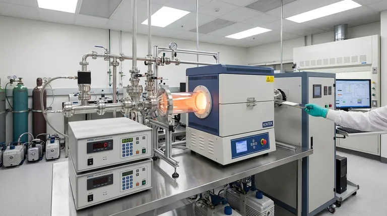
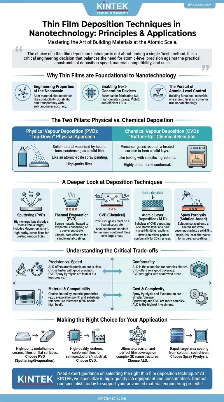
In nanotechnology, the primary techniques for depositing thin films fall into two main categories: Physical Vapour Deposition (PVD) and Chemical Vapour Deposition (CVD). More advanced methods like Atomic Layer Deposition (ALD) offer even greater precision, enabling the creation of functional layers that are only a few atoms thick. These methods are fundamental for building everything from semiconductor chips to advanced optical coatings.
The choice of a thin film deposition technique is not about finding a single "best" method. It is a critical engineering decision that balances the need for atomic-level precision against the practical constraints of deposition speed, material compatibility, and cost.
Why Thin Films are Foundational to Nanotechnology
Before comparing techniques, it's essential to understand why controlling materials at this scale is so revolutionary. Thin film deposition isn't just about applying a coating; it's about fundamentally engineering a material's properties from the atoms up.
Engineering Properties at the Nanoscale
At the nanoscale, the properties of a material can change dramatically. By depositing a film with subnanometer accuracy, you can create surfaces with entirely new characteristics, such as enhanced durability, specific electrical conductivity, transparency, or scratch resistance, that are different from the bulk source material.
Enabling Next-Generation Devices
This level of control is the engine behind many modern technologies. Integrated circuits, high-density data storage, micro-electromechanical systems (MEMS), and efficient LEDs all rely on meticulously layered thin films. These techniques are integral to fabricating today's most advanced devices.
The Pursuit of Atomic-Level Control
True nanotechnology emerges when we can dictate the placement of atoms. Deposition techniques are the tools that allow us to approach this goal, building functional materials one layer—or even one atomic layer—at a time.
The Two Pillars: Physical vs. Chemical Deposition
Nearly all common techniques can be classified as either a physical or chemical process. Understanding this distinction is the first step in selecting the right method.
Physical Vapour Deposition (PVD): A "Top-Down" Physical Approach
PVD methods take a solid source material, turn it into a vapour through physical means (like heating or bombardment with ions), and transport that vapour onto a substrate where it condenses back into a solid film.
Think of it as an atomic-scale spray painting process. This method is renowned for producing high-purity films because it avoids complex chemical reactions.
Chemical Vapour Deposition (CVD): A "Bottom-Up" Chemical Reaction
CVD introduces precursor gases into a reaction chamber. These gases react or decompose on the surface of a heated substrate, leaving behind the desired solid material as a thin film.
This is more like baking. You introduce specific ingredients (gases) that react under the right conditions (heat) to create a new, solid layer on the surface. CVD is widely used for its ability to produce highly uniform and conformal films.
A Deeper Look at Deposition Techniques
Within the PVD and CVD families, several specific methods are used, each with distinct advantages.
Sputtering (PVD): The High-Purity Workhorse
In sputtering, the source material (a "target") is bombarded with high-energy ions, which physically dislodge atoms from the target. These ejected atoms then travel and deposit onto the substrate.
Magnetron sputtering, a common variant, uses magnetic fields to trap electrons near the target, increasing the efficiency of the sputtering process. It is prized for its ability to create dense, high-purity films and effectively coat nanoparticles.
Thermal Evaporation (PVD): Simple and Direct
This is one of the simplest PVD methods. The source material is heated in a high vacuum until it evaporates, and the resulting vapour stream condenses on a cooler substrate. It is effective for depositing a wide range of metals but offers less control over film structure compared to sputtering.
Chemical Vapour Deposition (CVD): The Semiconductor Standard
CVD is the dominant technique in the semiconductor industry for good reason. It excels at producing extremely uniform films over large areas and can conform well to the topography of a surface. Its precision is a key reason for its use in creating the complex, multi-layered structures found in microchips.
Atomic Layer Deposition (ALD): The Ultimate in Precision
ALD is a subclass of CVD that offers the highest level of control possible. It deposits material one single atomic layer at a time by using a sequence of self-limiting chemical reactions.
This process allows for unparalleled conformality, enabling uniform coating of highly complex, 3D nanostructures with sub-nanometer precision. While slow, it is the go-to method when absolute perfection is required.
Spray Pyrolysis: A Solution-Based Alternative
This technique deviates from the vacuum-based methods. A solution containing the desired material is sprayed as a fine mist onto a heated substrate. The droplets undergo thermal decomposition (pyrolysis), leaving behind a solid film. It is often a lower-cost, higher-speed alternative for applications where absolute precision is less critical, such as in some photovoltaic solar cells.
Understanding the Critical Trade-offs
No single technique is superior in all aspects. The right choice depends on balancing four key factors for your specific goal.
Precision vs. Speed
There is a direct trade-off here. ALD offers atomic-layer precision but is exceptionally slow. CVD offers excellent precision and is faster than ALD. PVD methods and Spray Pyrolysis are generally the fastest but offer less control over film structure and thickness.
Conformality: Coating Complex Shapes
Conformality is the ability of a film to uniformly coat an uneven surface. ALD is the undisputed champion, providing perfect coverage on deep trenches and complex 3D structures. CVD also offers very good conformality. PVD, being a line-of-sight process, struggles to coat shadowed areas effectively.
Material and Substrate Compatibility
The choice of technique is often dictated by the materials involved. Some materials are difficult to evaporate or sputter (limiting PVD), while others may lack suitable chemical precursors (limiting CVD/ALD). Substrate temperature tolerance is also a major factor, as CVD processes often require high heat.
Cost and Complexity
System complexity and operational cost vary widely. Spray Pyrolysis and Thermal Evaporation systems are relatively simple and inexpensive. Sputtering and CVD systems are more complex and costly, while ALD systems represent the highest level of investment in both equipment and process time.
Making the Right Choice for Your Application
Use your primary goal to guide your decision on which deposition family to investigate further.
- If your primary focus is high-purity metal or simple ceramic films on flat surfaces: PVD techniques like sputtering or evaporation are your most effective and economical choices.
- If your primary focus is high-quality, uniform, and conformal films for semiconductor or industrial production: CVD is the established industry standard and provides a great balance of performance and throughput.
- If your primary focus is ultimate precision and perfect film coverage on complex 3D nanostructures: ALD is the only technique that can deliver the required atomic-level control, despite its slow speed.
- If your primary focus is rapid, large-area coating from a solution where cost is a major driver: Spray Pyrolysis offers a viable, high-speed alternative for applications like solar cells or certain sensors.
Understanding the fundamental principles and trade-offs of these techniques empowers you to select the precise tool needed to engineer materials at the nanoscale.
Summary Table:
| Technique | Category | Key Advantage | Ideal For |
|---|---|---|---|
| Sputtering | PVD | High-purity, dense films | Coating flat surfaces with metals/ceramics |
| Thermal Evaporation | PVD | Simple, cost-effective | Rapid metal deposition on simple substrates |
| CVD | Chemical | Uniform, conformal films | Semiconductor and industrial production |
| ALD | CVD (Advanced) | Atomic-layer precision | Perfect coating on complex 3D nanostructures |
| Spray Pyrolysis | Solution-based | Rapid, large-area coating | Low-cost applications like solar cells |
Need expert guidance on selecting the right thin film deposition technique for your lab? At KINTEK, we specialize in providing high-quality lab equipment and consumables tailored to your nanotechnology needs. Whether you require the precision of an ALD system, the reliability of a CVD setup, or the efficiency of PVD tools, our solutions are designed to enhance your research and production outcomes. Contact our specialists today to discuss how we can support your laboratory's advanced material engineering projects!
Visual Guide
Related Products
- Aluminized Ceramic Evaporation Boat for Thin Film Deposition
- Tungsten Evaporation Boat for Thin Film Deposition
- Electron Beam Evaporation Coating Oxygen-Free Copper Crucible and Evaporation Boat
- Molybdenum Tungsten Tantalum Evaporation Boat for High Temperature Applications
- Vacuum Hot Press Furnace Machine for Lamination and Heating
People Also Ask
- What is the widely used boat made of in thermal evaporation? Choosing the Right Material for High-Purity Deposition
- What is thin film deposition? Unlock Advanced Surface Engineering for Your Materials
- Why is an alumina boat and Ti3AlC2 powder bed necessary for Ti2AlC sintering? Protect MAX Phase Purity
- What are thin films deposited by evaporation? A Guide to High-Purity Coating
- What are the applications of thin films deposition? Unlock New Possibilities for Your Materials


