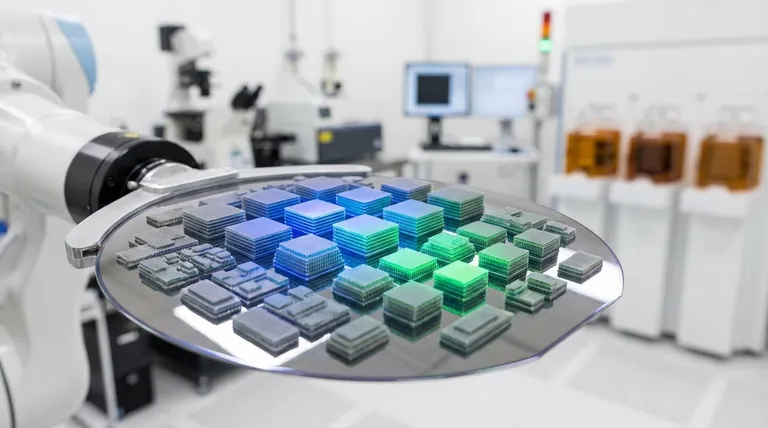
The primary uses of atomic layer deposition (ALD) are in fabricating high-performance microelectronics, advanced optics, and energy devices where creating ultra-thin, perfectly uniform, and defect-free films is critical. It is the go-to technology for coating complex, three-dimensional nanostructures, a task where other deposition methods fail. Key applications include manufacturing the gate dielectrics in modern computer chips, creating protective barriers for OLED displays, and improving the efficiency of solar cells.
Atomic layer deposition is not chosen for its speed, but for its unparalleled control. Its unique, self-limiting chemical process allows for the deposit of a material one single atomic layer at a time, guaranteeing exceptional film quality and the ability to perfectly coat even the most intricate surfaces.
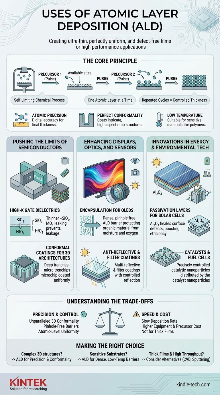
The Core Principle: Why ALD is Different
To understand its uses, you must first understand its mechanism. Unlike other techniques that continuously "spray" material onto a surface, ALD is a cyclical process.
A Two-Step, Self-Limiting Reaction
Each ALD cycle consists of two sequential chemical pulses. The first precursor gas is pulsed into the chamber and reacts with the surface until every available reaction site is occupied. This is the self-limiting step; no more material can be deposited.
The chamber is then purged, and a second precursor gas is introduced. This second precursor reacts only with the first layer, completing the deposition of a single, uniform monolayer of the desired material. This cycle is repeated to build the film layer by layer.
The Three Defining Characteristics
This unique process gives ALD three key advantages that dictate its applications:
- Atomic Precision: You control the final thickness with digital accuracy simply by counting the number of cycles.
- Perfect Conformality: Because the precursor gases can reach every part of a surface, ALD can coat extremely complex, high-aspect-ratio structures with perfect uniformity.
- Low Temperature: Many ALD processes can be run at relatively low temperatures, making it suitable for coating sensitive materials like polymers or organic electronics.
Application 1: Pushing the Limits of Semiconductors
The semiconductor industry is arguably the largest driver of ALD technology. As transistors shrink to the nanometer scale, traditional deposition methods are no longer sufficient.
High-k Gate Dielectrics
In modern transistors, a thin insulating layer called the gate dielectric prevents current leakage. As transistors got smaller, this layer had to become just a few atoms thick, but traditional silicon dioxide (SiO₂) began to leak.
ALD solved this by depositing new high-k materials (like HfO₂) with atomic precision. This allows for a physically thicker, more robust insulating layer that has the same electrical properties as a much thinner SiO₂ layer, enabling Moore's Law to continue.
Conformal Coatings for 3D Architectures
Modern devices rely on 3D structures like FinFETs (transistors with a vertical fin) and 3D NAND flash memory (which stacks memory cells vertically).
These structures contain deep, narrow trenches that are impossible to coat uniformly with conventional methods. ALD's perfect conformality ensures that the entire 3D surface, from the top to the very bottom, is coated with a film of the exact same thickness.
Application 2: Enhancing Displays, Optics, and Sensors
ALD's precision and low-temperature capabilities are ideal for creating advanced optical and protective coatings.
Encapsulation for OLEDs and Flexible Electronics
Organic Light-Emitting Diodes (OLEDs) and other flexible electronics are extremely sensitive to moisture and oxygen. Even a microscopic pinhole in a protective barrier can lead to device failure.
ALD creates exceptionally dense and pinhole-free barrier films at low temperatures, perfectly encapsulating the sensitive organic materials without damaging them. This dramatically increases the lifetime and reliability of OLED displays.
Anti-Reflective and Filter Coatings
For high-performance lenses, sensors, and solar cells, controlling the reflection and transmission of light is critical.
ALD allows for the creation of complex stacks of different materials with precise thickness control. This enables the fabrication of highly effective anti-reflective (AR) coatings and optical filters that are perfectly uniform across the entire surface.
Application 3: Innovations in Energy and Environmental Tech
ALD is a key enabling technology for next-generation batteries, solar cells, and catalysts.
Passivation Layers for Solar Cells
Minor defects on the surface of a silicon wafer can trap electrons, reducing the efficiency of a solar cell.
ALD is used to deposit an ultra-thin "passivation" layer (often aluminum oxide, Al₂O₃) that chemically "heals" these surface defects. This simple step significantly boosts the efficiency and power output of high-performance solar cells.
Catalysts and Fuel Cells
The performance of a catalyst often depends on having very small, precisely controlled nanoparticles distributed over a large surface area.
ALD allows for the direct synthesis of these catalytic nanoparticles with exact control over their size and composition, leading to more efficient and durable catalysts for industrial processes and fuel cells.
Understanding the Trade-offs: Precision vs. Speed
Despite its powerful advantages, ALD is not the right solution for every problem. Its primary limitation is a direct consequence of its core strength.
The Major Drawback: Slow Deposition Rate
Because it builds a film one atomic layer at a time, ALD is an inherently slow process. Its deposition rates are often orders of magnitude lower than those of techniques like Chemical Vapor Deposition (CVD) or Physical Vapor Deposition (PVD).
Cost and Complexity
ALD systems and the high-purity precursor chemicals they require can be more expensive than conventional deposition equipment. This makes it a high-value tool reserved for applications where its unique capabilities are non-negotiable.
When to Choose an Alternative
If your application simply requires a thick film (microns or more) on a relatively flat surface, and atomic-level uniformity is not a primary concern, ALD is likely overkill. Faster and more cost-effective methods like sputtering or CVD would be more appropriate.
Making the Right Choice for Your Goal
Deciding whether to use ALD requires evaluating the trade-off between its unparalleled precision and its slow speed.
- If your primary focus is atomic-level control and perfect 3D conformality: ALD is the definitive choice for coating complex nanostructures in advanced electronics and MEMS.
- If your primary focus is creating dense, pinhole-free barriers on sensitive substrates: ALD's ability to create high-quality films at low temperatures makes it ideal for encapsulating OLEDs, polymers, and medical implants.
- If your primary focus is high-throughput, thick-film deposition: You should strongly consider alternative methods like CVD or sputtering, as ALD's slow deposition rate will be a significant bottleneck.
Ultimately, atomic layer deposition is the essential manufacturing tool for applications where absolute control over thickness, uniformity, and material quality is the most critical factor.
Summary Table:
| Application Area | Key Use of ALD | Key Materials/Structures |
|---|---|---|
| Semiconductors | High-k gate dielectrics, 3D NAND, FinFETs | HfO₂, Conformal coatings on trenches |
| Displays & Optics | OLED encapsulation, Anti-reflective coatings | Pinhole-free barriers, Optical filter stacks |
| Energy & Environment | Solar cell passivation, Catalyst synthesis | Al₂O₃, Nanoparticles for fuel cells |
Need to deposit ultra-thin, uniform films on complex nanostructures? KINTEK specializes in lab equipment and consumables, providing advanced ALD solutions for semiconductor, optics, and energy research. Our technology ensures atomic-level precision and perfect conformality for your most demanding applications. Contact us today to enhance your lab's capabilities with reliable, high-performance ALD systems!
Visual Guide
Related Products
- RF PECVD System Radio Frequency Plasma-Enhanced Chemical Vapor Deposition RF PECVD
- Chemical Vapor Deposition CVD Equipment System Chamber Slide PECVD Tube Furnace with Liquid Gasifier PECVD Machine
- Electron Beam Evaporation Coating Oxygen-Free Copper Crucible and Evaporation Boat
- Hemispherical Bottom Tungsten Molybdenum Evaporation Boat
- HFCVD Machine System Equipment for Drawing Die Nano-Diamond Coating
People Also Ask
- Why is a Matching Network Indispensable in RF-PECVD for Siloxane Films? Ensure Stable Plasma and Uniform Deposition
- What is an example of PECVD? RF-PECVD for High-Quality Thin Film Deposition
- What is plasma enhanced chemical vapour deposition process? Unlock Low-Temperature, High-Quality Thin Films
- What is the role of RF-PECVD in VFG preparation? Mastering Vertical Growth and Surface Functionality
- How does Radio Frequency Enhanced Plasma Chemical Vapour Deposition (RF-PECVD) work? Learn the Core Principles


