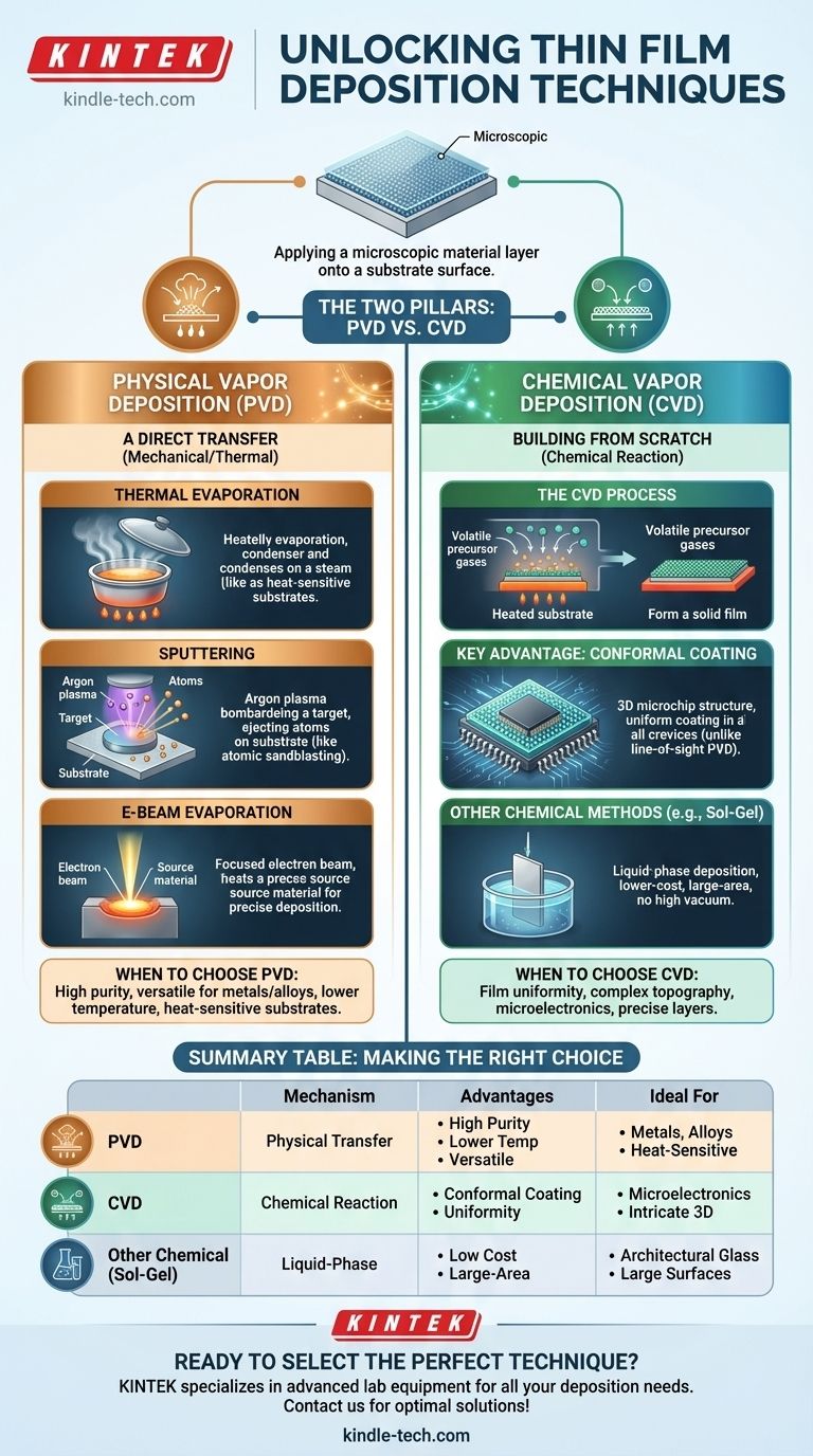
In essence, thin film deposition is the process of applying a microscopic layer of material onto a surface, known as a substrate. These techniques are categorized into two primary families based on their core mechanism: those that physically transfer material and those that create the material through a chemical reaction on the substrate surface. The chosen method is critical, as it fundamentally determines the final properties of the film, from its purity to its structural integrity.
The decision between deposition techniques is not about finding a single "best" method. It is about matching the process—either a physical transfer or a chemical creation—to the specific material, substrate, and performance requirements of the final product.
The Two Pillars of Deposition: PVD vs. CVD
At the highest level, deposition techniques are split into Physical Vapor Deposition (PVD) and Chemical Vapor Deposition (CVD).
The fundamental difference is simple: PVD is a mechanical or thermal process that moves atoms from a source to the substrate, like spray painting. CVD is a chemical process where precursor gases react on the substrate's surface to grow the film from scratch.
Physical Vapor Deposition (PVD): A Direct Transfer
PVD encompasses methods that transport a solid material into a vapor phase within a vacuum, which then condenses onto a substrate to form the thin film.
Thermal Evaporation
This is one of the simplest PVD methods. A source material is heated in a high vacuum chamber until it evaporates. These gaseous atoms travel in a straight line and condense on the cooler substrate, forming the film.
Think of it like boiling a pot of water and seeing steam condense on a cold lid held above it.
Sputtering
Sputtering is a more energetic process. Instead of heat, it uses a plasma of an inert gas, like argon. High-energy ions from this plasma are accelerated to strike a solid "target" of the desired material.
This bombardment acts like an atomic-scale sandblaster, ejecting or "sputtering" atoms from the target, which then coat the substrate. This method offers excellent control over film composition.
Electron Beam (E-Beam) Evaporation
A more precise variant of thermal evaporation, E-beam evaporation uses a focused beam of high-energy electrons to heat the source material. This allows for the deposition of materials with very high melting points and provides greater control over the evaporation rate.
Chemical Vapor Deposition (CVD): Building from Scratch
CVD does not transfer existing material. Instead, it involves building the film directly on the substrate through a controlled chemical reaction.
The CVD Process
In a CVD process, one or more volatile precursor gases are introduced into a reaction chamber. When these gases come into contact with the heated substrate, they react or decompose, leaving behind a solid material that forms the thin film.
Key Advantage: Conformal Coating
Because the film is grown via a surface chemical reaction, CVD excels at creating highly uniform (conformal) coatings. It can evenly coat complex, three-dimensional surfaces with high precision, which is something line-of-sight PVD methods struggle with. This makes it indispensable in the semiconductor industry for creating intricate layered structures on microchips.
Understanding the Trade-offs
Choosing the right technique requires understanding the inherent strengths and weaknesses of each approach.
When to Choose PVD
PVD is often preferred for depositing high-purity coatings of metals, alloys, and simple compounds. Since it is often a lower-temperature process than CVD, it can be used on substrates that are sensitive to heat. Sputtering, in particular, is highly versatile for creating films from a wide range of materials.
When to Choose CVD
CVD is the superior choice when film uniformity and step coverage on complex topography are critical. Its ability to produce highly conformal layers makes it the standard for many advanced semiconductor and optical coating applications where precision is paramount.
Other Chemical Methods
Beyond CVD, other liquid-phase chemical methods exist, such as sol-gel and chemical bath deposition. These involve dipping the substrate into a chemical solution or coating it with a gel, which is then dried and cured to form the film. These are often lower-cost and do not require high-vacuum systems, making them suitable for large-area applications like coating architectural glass.
Making the Right Choice for Your Application
Your goal dictates the optimal technology. There is no single solution; instead, the correct choice is a function of your specific technical and commercial needs.
- If your primary focus is high purity and versatility for metals or simple compounds: PVD techniques like sputtering are often the most direct and effective choice.
- If your primary focus is creating a highly uniform, conformal coating on a complex surface: CVD is unmatched for its precision and is the standard in fields like microelectronics.
- If your primary focus is low-cost, large-area coating without high-vacuum requirements: Liquid-phase chemical methods like sol-gel or spray pyrolysis can be a practical alternative.
Ultimately, understanding these fundamental principles empowers you to select a deposition technique not just for what it is, but for what it can achieve for your specific goal.
Summary Table:
| Technique | Mechanism | Key Advantages | Ideal For |
|---|---|---|---|
| PVD (Physical Vapor Deposition) | Physical transfer of material via vapor phase | High purity, lower temperature, versatile for metals | Metals, alloys, heat-sensitive substrates |
| CVD (Chemical Vapor Deposition) | Chemical reaction on substrate surface | Conformal coating, uniform layers on complex shapes | Microelectronics, intricate 3D structures |
| Other Chemical Methods (e.g., Sol-Gel) | Liquid-phase deposition | Low cost, large-area coating, no vacuum required | Architectural glass, large surfaces |
Ready to select the perfect thin film deposition technique for your project?
At KINTEK, we specialize in providing advanced lab equipment and consumables for all your deposition needs. Whether you require high-purity PVD systems for metal coatings or precise CVD solutions for semiconductor applications, our experts can help you achieve optimal results.
Contact us today to discuss your specific requirements and discover how KINTEK's solutions can enhance your laboratory's capabilities and drive your research forward.
Visual Guide
Related Products
- Aluminized Ceramic Evaporation Boat for Thin Film Deposition
- Tungsten Evaporation Boat for Thin Film Deposition
- Electron Beam Evaporation Coating Oxygen-Free Copper Crucible and Evaporation Boat
- Molybdenum Tungsten Tantalum Evaporation Boat for High Temperature Applications
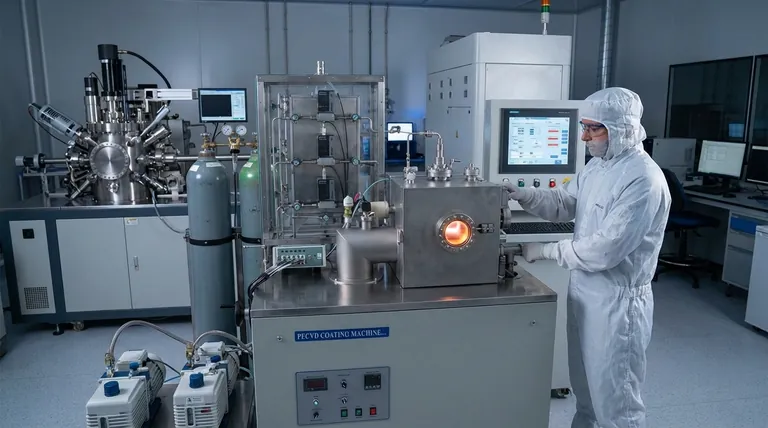
- HFCVD Machine System Equipment for Drawing Die Nano-Diamond Coating
People Also Ask
- What are the alternatives to sputtering? Choose the Right Thin Film Deposition Method
- What is the source of evaporation for thin film? Choosing Between Thermal and E-Beam Methods
- What is the widely used boat made of in thermal evaporation? Choosing the Right Material for High-Purity Deposition
- Why are high-purity ceramic boats used for lignin activation? Ensure Purity & Thermal Stability
- What are thin films deposited by evaporation? A Guide to High-Purity Coating


