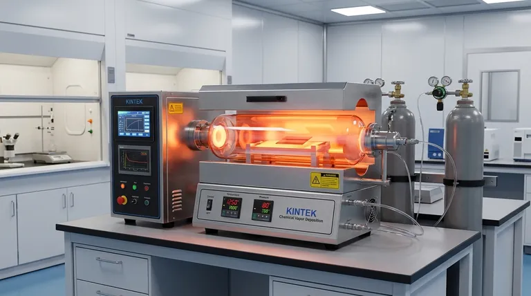
In advanced materials science, a Chemical Vapor Deposition (CVD) reactor is a highly controlled chamber where gaseous chemical precursors react to form a solid, high-purity film on a substrate's surface. It is not merely an oven, but a precision instrument that meticulously manages temperature, pressure, and gas flow to build materials, often one atomic layer at a time. This process is fundamental to producing the high-performance components used in semiconductors, protective coatings, and even lab-grown diamonds.
At its core, a CVD reactor is an environment engineered for atomic-level construction. Its purpose is to create the exact conditions necessary for gas molecules to break apart and deposit onto a surface, forming a new solid material with exceptional purity and uniformity.
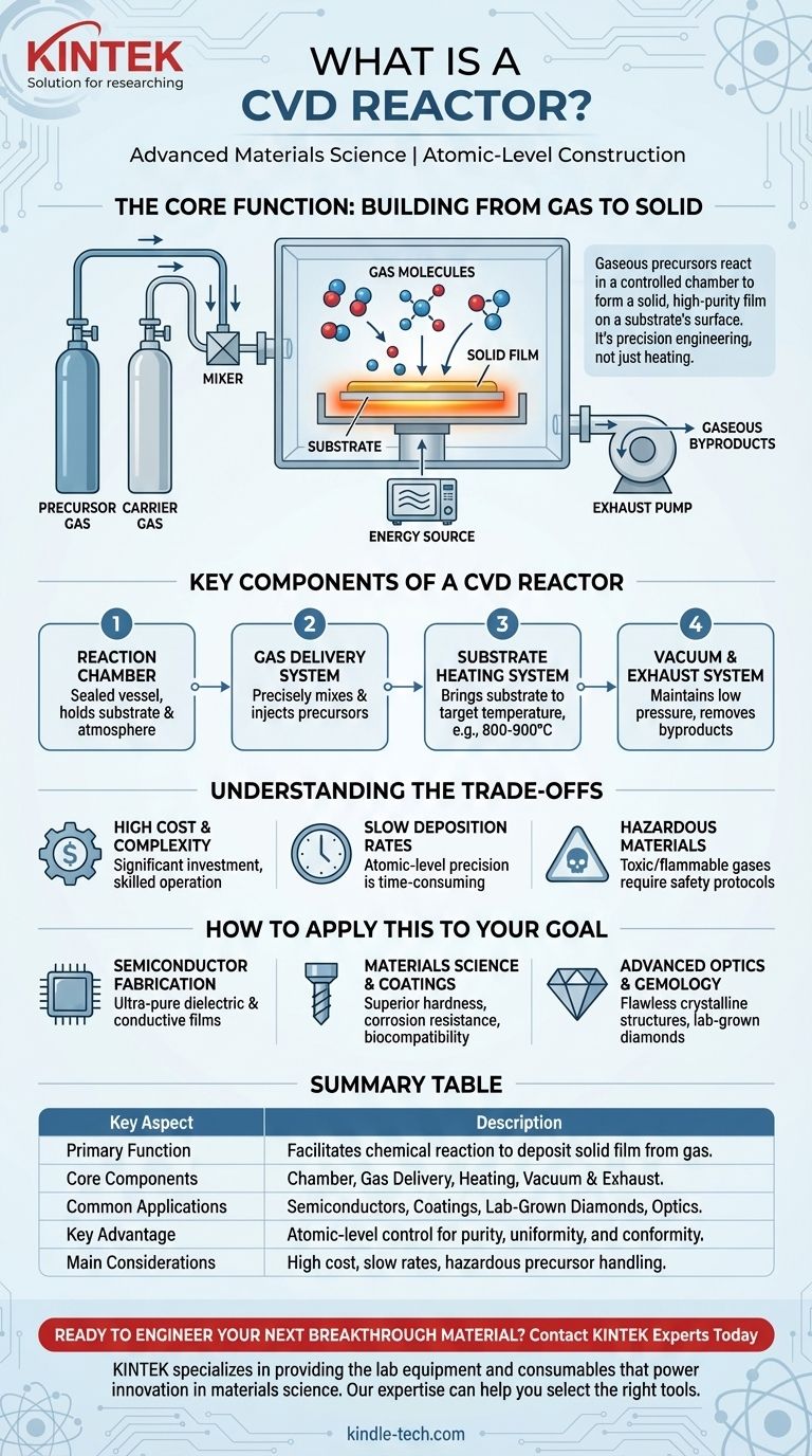
The Core Function: Building from Gas to Solid
A CVD reactor's primary job is to facilitate a specific chemical reaction. It creates an environment where a volatile precursor—a gas containing the atoms you want to deposit—can be introduced, activated, and then grown into a solid layer on a target object, known as a substrate.
The Principle of Deposition
The process begins by introducing carefully measured precursor gases into the reactor chamber. For example, to create a silicon film, a gas like silane (SiH₄) would be used. To grow a diamond, a carbon-rich gas like methane (CH₄) is required.
The Role of Energy and Heat
The substrate inside the chamber is heated to a precise, high temperature, often between 800°C and 900°C. This heat provides the energy needed for the chemical reactions to occur on the substrate's surface. In many systems, an additional energy source like microwaves or lasers is used to ionize the gas into a plasma, which dramatically speeds up the process.
The Substrate as a Foundation
The substrate is the foundation upon which the new material is built. This could be a silicon wafer in semiconductor manufacturing or a tiny diamond "seed" for growing a larger gem. The gas molecules react on this heated surface, depositing a thin, solid film that conforms perfectly to the substrate.
The Result: A High-Purity Film
As the precursor gases decompose and react, they leave behind a solid layer of the desired material. The gaseous byproducts are pumped out of the chamber. The result is an exceptionally pure and uniform film with precisely controlled thickness and properties, which is why CVD is essential for high-tech applications.
Key Components of a CVD Reactor
While designs vary based on the application, nearly all CVD reactors share a common set of critical systems that work in concert.
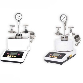
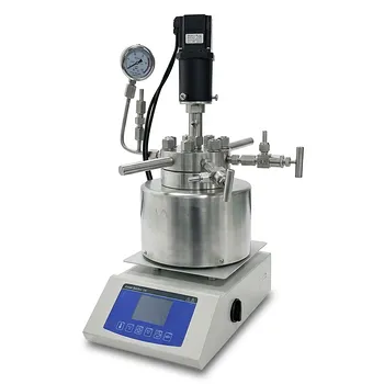
The Reaction Chamber
This is the heart of the reactor—a sealed vessel, typically made of quartz or stainless steel, that can withstand high temperatures and vacuum conditions. It contains the substrate and the reactive gas atmosphere.
Gas Delivery System
This network of pipes, valves, and mass flow controllers acts as the reactor's circulatory system. It precisely mixes and injects precursor and carrier gases into the chamber at controlled rates, ensuring the chemical "recipe" is exact.
Substrate Heating System
This component, often a resistive heater or induction coil, brings the substrate to the target reaction temperature. Uniform heating is critical for producing a uniform film across the entire substrate surface.
Vacuum & Exhaust System
A powerful vacuum pump is used to remove air from the chamber before the process begins, ensuring purity. During deposition, it removes unreacted gases and chemical byproducts, maintaining the low pressure and controlled atmosphere necessary for the reaction.
Understanding the Trade-offs
While powerful, CVD technology involves significant challenges and is not a universal solution for all manufacturing needs.
High Cost and Complexity
CVD reactors are sophisticated and expensive pieces of equipment. They require significant capital investment and skilled technicians to operate and maintain, given the precise control needed over multiple variables.
Slow Deposition Rates
Building materials with atomic-level precision is inherently slow. Growing a single lab-grown diamond can take days or weeks, and producing films for semiconductors is a meticulous, time-consuming step in the overall fabrication process.
Hazardous Materials
The precursor gases used in CVD are often toxic, flammable, or corrosive. This necessitates extensive safety protocols, specialized handling equipment, and robust exhaust management systems to protect operators and the environment.
How to Apply This to Your Goal
Understanding the function of a CVD reactor helps you recognize its role as a foundational tool in modern technology.
- If your primary focus is semiconductor fabrication: A CVD reactor is the critical instrument for creating the ultra-pure, nanometer-scale dielectric and conductive films that define the performance of microchips.
- If your primary focus is materials science and coatings: This technology is your method for engineering surfaces with superior hardness, corrosion resistance, or biocompatibility for tools, medical implants, and automotive parts.
- If your primary focus is advanced optics or gemology: The reactor is what enables the growth of flawless crystalline structures, like artificial diamonds or specialized optical components, that are impossible to create with traditional methods.
Ultimately, a CVD reactor is not just a piece of equipment; it is the engine that enables innovation wherever the properties of a material's surface are paramount.
Summary Table:
| Key Aspect | Description |
|---|---|
| Primary Function | Facilitates a chemical reaction to deposit a solid, high-purity film from gaseous precursors onto a substrate. |
| Core Components | Reaction Chamber, Gas Delivery System, Substrate Heating System, Vacuum & Exhaust System. |
| Common Applications | Semiconductor fabrication, Protective & Functional Coatings, Lab-Grown Diamonds, Advanced Optics. |
| Key Advantage | Enables atomic-level control for exceptional material purity, uniformity, and conformity. |
| Main Considerations | High equipment cost, slow deposition rates, and requires handling of hazardous precursor gases. |
Ready to Engineer Your Next Breakthrough Material?
Whether you are developing next-generation semiconductors, advanced protective coatings, or high-purity crystalline materials, the precision of a CVD reactor is critical. KINTEK specializes in providing the lab equipment and consumables that power innovation in materials science.
Our expertise can help you select the right tools to achieve the atomic-level control your research demands. Contact our experts today to discuss how we can support your laboratory's specific needs and accelerate your path to discovery.
Visual Guide
Related Products
- Cylindrical Resonator MPCVD Machine System Reactor for Microwave Plasma Chemical Vapor Deposition and Lab Diamond Growth
- Customer Made Versatile CVD Tube Furnace Chemical Vapor Deposition Chamber System Equipment
- Microwave Plasma Chemical Vapor Deposition MPCVD Machine System Reactor for Lab and Diamond Growth
- 915MHz MPCVD Diamond Machine Microwave Plasma Chemical Vapor Deposition System Reactor
- Split Chamber CVD Tube Furnace with Vacuum Station Chemical Vapor Deposition System Equipment Machine
People Also Ask
- What pressure is needed for chemical vapor deposition of diamonds? Master the Low-Pressure 'Sweet Spot'
- How are CVD diamonds created? Discover the Science of Lab-Grown Diamond Precision
- Why is argon-rich gas phase chemistry used for UNCD growth? Unlock Precision Nano-Diamond Synthesis
- What is the difference between MPCVD and HFCVD? Choose the Right CVD Method for Your Application
- What are the primary advantages of the CVD method for growing diamonds? Engineering High-Purity Gems and Components