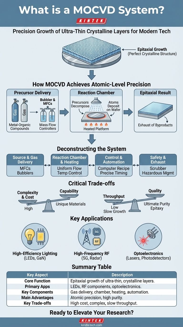
In simplest terms, a MOCVD system is a highly sophisticated machine designed to grow ultra-thin, perfectly ordered crystalline layers of material on a substrate. Its full name, Metal-Organic Chemical Vapor Deposition (MOCVD), describes its process of using metal-organic compounds in gas form to deposit atoms with extreme precision. This technology is the fundamental manufacturing tool for modern LEDs, high-frequency RF components, and advanced optoelectronics.
The true purpose of a MOCVD system is not just to deposit material, but to achieve epitaxial growth—a perfectly ordered crystalline structure that mimics the substrate below. This is accomplished by reacting volatile precursor gases in a highly controlled environment, making MOCVD a cornerstone of high-performance semiconductor fabrication.
How MOCVD Achieves Atomic-Level Precision
The magic of MOCVD lies in its ability to precisely control a chemical reaction on a wafer's surface. The entire process is a carefully choreographed sequence designed to build materials one atomic layer at a time.
The Core Principle: Chemical Vapor Deposition
At its heart, the process involves injecting precisely measured amounts of pure gases, known as precursors, into a reaction chamber. These precursors are special "metal-organic" compounds, which contain the desired metal atoms (like gallium or indium) attached to organic molecules.
Delivering the Precursors
The system uses a bubbler to turn the liquid metal-organic sources into a gas. A carrier gas (like hydrogen or nitrogen) is bubbled through the liquid source, picking up a predictable concentration of the source material vapor.
This gas mixture then travels through a network of pipes and valves, managed by mass flow controllers that ensure the exact desired amount reaches the reaction chamber.
The Reaction Chamber: Where Growth Happens
Inside the chamber, a wafer substrate sits on a heated platform. When the precursor gases flow over this hot surface, they undergo a chemical reaction and decompose.
This reaction frees the metal atoms, which then deposit onto the wafer's surface. The leftover organic molecules and other byproducts are carried away by the gas stream and removed from the chamber.
The Result: Epitaxial Growth
Because this process is so slow and controlled, the deposited atoms arrange themselves to follow the crystal structure of the underlying wafer. This is called epitaxial growth.
The result is an exceptionally pure, defect-free crystalline film. This perfect structure is what gives the final semiconductor device its high performance. The process is sometimes called Metal-Organic Vapor Phase Epitaxy (MOVPE) to emphasize this outcome.
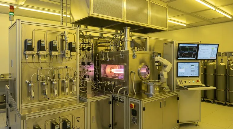
Deconstructing the MOCVD System
A modern MOCVD tool is a complex integration of several critical subsystems, all working in unison to maintain control over the growth process.
Source and Gas Delivery System
This is the system of bubblers, gas lines, and mass flow controllers (MFCs) that store, vaporize, and transport the precursor gases. Its single most important function is to deliver a stable, reproducible, and precise flow of reactants to the chamber.
Reaction Chamber and Heating System
This is the core of the machine where the wafer is processed. The chamber is designed for uniform gas flow and temperature distribution across the wafer, which is essential for growing consistent material layers. Precise temperature control is non-negotiable.
Control and Automation Systems
The entire growth process, or "recipe," is managed by a computer. This system controls every variable—gas flows, valve switching, temperature ramps, pressure, and timing—with split-second accuracy, ensuring the process is repeatable from run to run.
Safety and Exhaust Management
MOCVD precursors are often toxic, flammable, and pyrophoric (ignite on contact with air). A robust safety and alarm system is therefore critical. Additionally, a tail gas treatment system scrubs the exhaust gas to neutralize hazardous byproducts before they are vented.
Understanding the Critical Trade-offs
While powerful, MOCVD is a specialized technology with inherent trade-offs that make it suitable for specific applications.
Complexity vs. Capability
MOCVD systems are extremely complex and expensive. The requirement for high-purity gas handling, precise temperature and pressure control, and extensive safety systems results in high capital and maintenance costs. This complexity, however, is precisely what enables the growth of unique, high-performance materials that other methods cannot produce.
Throughput vs. Quality
Achieving perfect epitaxial layers is a slow, meticulous process. Growth rates are often measured in nanometers per minute. Therefore, MOCVD is not a high-throughput technology; it is optimized for ultimate material quality, not sheer volume.
Material and Safety Constraints
The process relies on a specific class of volatile and often hazardous metal-organic precursors. This reality constrains the types of materials that can be grown and imposes strict facility and safety protocols that add to the operational overhead.
Key Applications and Why MOCVD is Chosen
Understanding MOCVD's capabilities helps clarify why it is the indispensable tool for specific, demanding applications.
- If your primary focus is high-efficiency lighting (LEDs): MOCVD is essential for growing the complex III-V semiconductor layer structures (like Gallium Nitride, or GaN) that emit light efficiently.
- If your primary focus is high-frequency electronics (RF): MOCVD provides the high-purity, defect-free materials needed for the transistors in power amplifiers used for 5G and radar systems.
- If your primary focus is optoelectronics (lasers, photodetectors): MOCVD's precise control over layer thickness and composition is critical for fabricating the multi-layered structures that generate and detect light.
Ultimately, a MOCVD system is a tool of atomic-scale construction, enabling the creation of the fundamental materials that power our modern technological world.
Summary Table:
| Key Aspect | Description |
|---|---|
| Core Function | Epitaxial growth of ultra-thin, crystalline layers on a substrate |
| Primary Applications | LEDs, high-frequency RF components, lasers, photodetectors |
| Key Components | Gas delivery system, reaction chamber, heating system, control automation |
| Main Advantages | Atomic-level precision, high material purity, complex layer structures |
| Key Trade-offs | High cost, complex operation, slower throughput for superior quality |
Ready to Elevate Your Semiconductor Research or Production?
KINTEK specializes in providing advanced lab equipment and consumables for cutting-edge semiconductor fabrication. Whether you're developing next-generation LEDs, high-frequency RF components, or optoelectronic devices, our expertise in MOCVD technology can help you achieve unparalleled material quality and device performance.
Contact us today to discuss how our solutions can support your laboratory's specific needs and drive your innovations forward.
Visual Guide
Related Products
- 915MHz MPCVD Diamond Machine Microwave Plasma Chemical Vapor Deposition System Reactor
- Multi Heating Zones CVD Tube Furnace Machine Chemical Vapor Deposition Chamber System Equipment
- Microwave Plasma Chemical Vapor Deposition MPCVD Machine System Reactor for Lab and Diamond Growth
- Cylindrical Resonator MPCVD Machine System Reactor for Microwave Plasma Chemical Vapor Deposition and Lab Diamond Growth
- Customer Made Versatile CVD Tube Furnace Chemical Vapor Deposition Chamber System Equipment
People Also Ask
- How is a diamond formed from CVD? The Science of Growing Diamonds Atom by Atom
- How are CVD diamonds created? Discover the Science of Lab-Grown Diamond Precision
- Why is MW-CVD preferred for high-purity diamond optical windows? Achieve Zero-Contamination Material Growth
- How do vacuum pumps and valves collaborate in MPCVD? Achieve Precise Pressure Control for Superior CNT Synthesis
- What is microwave plasma CVD? A Guide to High-Purity Diamond and Material Synthesis


