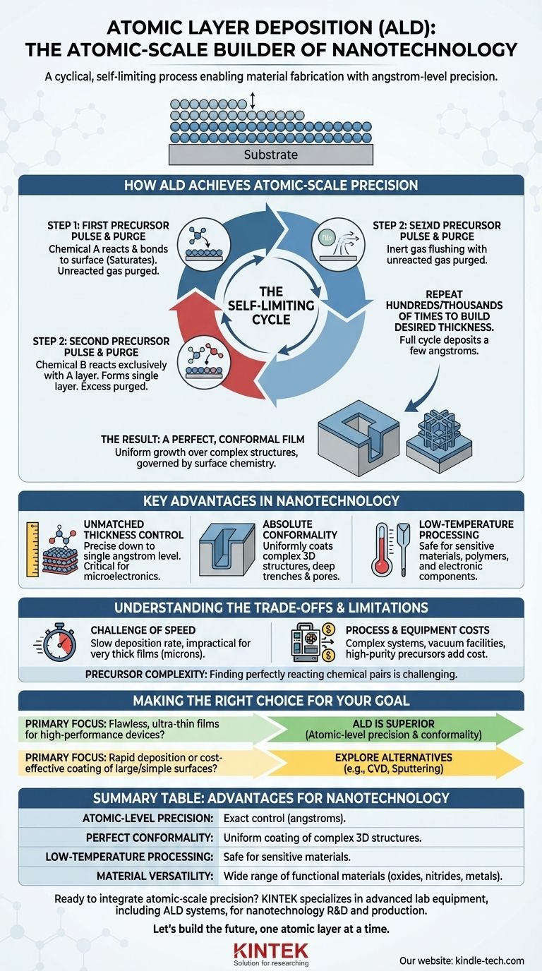
Atomic Layer Deposition (ALD) is a cornerstone of modern nanotechnology, enabling the fabrication of materials with atomic-scale precision. It is a thin-film deposition technique that builds films one single layer of atoms at a time through a sequence of self-limiting, gas-phase chemical reactions. This meticulous process provides unparalleled control over film thickness and composition.
The core principle of ALD is its unique, cyclical nature. Unlike methods that deposit material continuously, ALD uses alternating pulses of chemical precursors, ensuring that each reaction completes fully across the surface before the next begins. This self-limiting behavior is the key to its precision and its power in creating nanoscale devices.
How ALD Achieves Atomic-Scale Precision
The power of ALD lies in its carefully controlled, two-step reaction cycle. This process is repeated hundreds or thousands of times to build a film of the desired thickness.
The Self-Limiting Cycle
At the heart of ALD is a "self-limiting" reaction. This means the chemical reaction naturally stops after a single, complete atomic layer has formed on the substrate.
Step 1: First Precursor Pulse and Purge
First, a gas-phase precursor (Chemical A) is pulsed into the reaction chamber. The precursor molecules react with and bond to the surface of the substrate until all available reactive sites are occupied.
Once the surface is saturated, any excess, unreacted precursor gas is removed from the chamber with an inert gas purge.
Step 2: Second Precursor Pulse and Purge
Next, a second precursor (Chemical B) is introduced. This chemical reacts exclusively with the first precursor layer (Chemical A) that is now bonded to the surface, forming a single, stable layer of the desired material.
After this reaction is complete, the chamber is purged again to remove any excess of Chemical B and reaction byproducts. This full cycle typically deposits a film of just a few angstroms.
The Result: A Perfect, Conformal Film
By repeating this "A -> Purge -> B -> Purge" cycle, a film is built with atomic precision. Because the reactions are governed by surface chemistry rather than line-of-sight deposition, the film grows uniformly over even the most complex, three-dimensional nanoscale structures.
Key Advantages in Nanotechnology
ALD is not the fastest or cheapest method, but its specific advantages make it indispensable for demanding nanotechnology applications like advanced microelectronics and biomedical devices.
Unmatched Thickness Control
The ability to control film thickness down to the single angstrom level is critical for fabricating modern devices like MOSFET gate stacks and DRAM capacitors, where performance is dictated by atomic-scale dimensions.
Absolute Conformality
ALD provides a perfectly uniform coating that conforms to any shape. This is essential for coating the inside of deep trenches or complex 3D nanostructures found in next-generation memory and processing chips.
Low-Temperature Processing
The deposition can often be performed at relatively low temperatures. This allows for the coating of sensitive materials, such as polymers or fully fabricated electronic components, that would be damaged by higher-temperature processes.
Understanding the Trade-offs and Limitations
While powerful, ALD is a specialized tool with clear limitations that make it unsuitable for all applications. Understanding these trade-offs is crucial for making an informed decision.
The Challenge of Speed
The primary drawback of ALD is its slow deposition rate. Building a film one atomic layer at a time is inherently time-consuming, making it impractical for applications that require very thick films (many microns).
Process and Equipment Costs
ALD systems are complex and require expensive vacuum facilities. The need for high-purity precursors and precise process control adds to the overall operational cost.
Precursor Chemistry Complexity
Developing a reliable ALD process requires finding two precursor chemicals that react perfectly with each other and the substrate, but not with themselves. This chemistry can be challenging and is not available for all materials.
Making the Right Choice for Your Goal
Selecting ALD depends entirely on whether your application demands atomic-level control over its material properties.
- If your primary focus is creating flawless, ultra-thin films for high-performance devices: ALD is the superior choice due to its atomic-level precision and conformality.
- If your primary focus is rapid deposition or coating large, simple surfaces cost-effectively: You should explore alternative methods like Chemical Vapor Deposition (CVD) or sputtering, as ALD's speed and cost will be significant drawbacks.
Ultimately, ALD grants engineers the power to design and build materials from the atom up, a defining capability in the world of nanotechnology.
Summary Table:
| Feature | Advantage for Nanotechnology |
|---|---|
| Atomic-Level Precision | Enables exact control of film thickness down to the angstrom level. |
| Perfect Conformality | Uniformly coats complex 3D nanostructures, trenches, and pores. |
| Low-Temperature Processing | Safe for coating sensitive materials like polymers and pre-fabricated components. |
| Material Versatility | Deposits a wide range of high-quality functional materials (oxides, nitrides, metals). |
Ready to integrate atomic-scale precision into your R&D or production line?
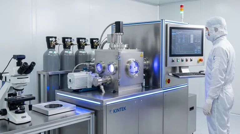
KINTEK specializes in advanced lab equipment, including ALD systems, to meet the demanding needs of nanotechnology research and development. Our solutions empower you to create flawless, conformal thin films essential for next-generation microelectronics, MEMS, and biomedical devices.
Contact us today to discuss how our expertise and reliable equipment can accelerate your innovation. Let's build the future, one atomic layer at a time.
Visual Guide
Related Products
- Chemical Vapor Deposition CVD Equipment System Chamber Slide PECVD Tube Furnace with Liquid Gasifier PECVD Machine
- RF PECVD System Radio Frequency Plasma-Enhanced Chemical Vapor Deposition RF PECVD
- HFCVD Machine System Equipment for Drawing Die Nano-Diamond Coating
- 915MHz MPCVD Diamond Machine Microwave Plasma Chemical Vapor Deposition System Reactor
- Inclined Rotary Plasma Enhanced Chemical Vapor Deposition PECVD Equipment Tube Furnace Machine
People Also Ask
- Why is Chemical Vapor Deposition (CVD) equipment uniquely suited for constructing hierarchical superhydrophobic structures?
- What are the processes of vapor phase deposition? Understand CVD vs. PVD for Superior Thin Films
- What is plasma enhanced chemical vapor deposition PECVD equipment? A Guide to Low-Temperature Thin Film Deposition
- What happens during deposition chemistry? Building Thin Films from Gaseous Precursors
- What are the advantages of chemical vapor deposition? Achieve Superior Thin Films for Your Lab


