All Questions
Why Is The Temperature Control Precision Critical For Bifeo3 Thin Film Synthesis? Achieve Pure Phase & Stoichiometry.
Discover why high-precision temperature control is essential for BiFeO3 thin film synthesis to prevent bismuth loss and ensure phase purity.
What Are The Advantages And Primary Use Of Hfcvd Systems? Master Diamond Film Production With Ease
Learn why HFCVD is the preferred method for diamond film growth, featuring simple operation, high growth rates, and complex geometry coating.
What Are The Advantages And Applications Of Laser Induced Chemical Vapour Deposition (Lcvd)? Precision Thin-Film Solutions
Explore the benefits of LCVD: low-temperature deposition, high purity, and complex geometry coating for semiconductors, diamonds, and nanotubes.
What Is Medium Temperature Chemical Vapour Deposition (Mtcvd) Used For? Enhance Tool Life & Performance
Learn how MTCVD technology creates dense, hard coatings for carbide tools, enabling high-speed, dry cutting and extending equipment service life.
What Are The Characteristics And Applications Of High Temperature Chemical Vapour Deposition (Htcvd)? Grow Bulk Sic Crystals
Learn how High Temperature Chemical Vapour Deposition (HTCVD) enables rapid Silicon Carbide crystal growth at temperatures up to 2300°C.
What Is Organometallic Chemical Vapour Deposition (Mocvd) Used For? Leading Led And Gan Semiconductor Growth
Learn how MOCVD enables epitaxial growth for LEDs, GaN semiconductors, and complex 3D coating applications with high precision and purity.
What Are The Characteristics And Applications Of Vapour Phase Epitaxy (Vpe)? Key Insights For Semiconductor Growth
Learn how Vapour Phase Epitaxy (VPE) produces high-purity semiconductors. Explore VPE characteristics, methodologies, and industrial applications.
What Are The Benefits And Applications Of Atomic Layer Chemical Vapour Deposition (Alcvd)? Unlock Atomic Precision
Learn how ALCVD (ALD) delivers atomic-level thickness control, superior conformality, and high-purity films for semiconductor and nano-applications.
What Are The Advantages And Applications Of Low Pressure Chemical Vapour Deposition (Lpcvd)? Expert Guide
Learn how LPCVD offers superior film uniformity, high purity, and batch efficiency for semiconductor manufacturing and advanced nanomaterials.
What Are The Characteristics And Applications Of Atmospheric Pressure Chemical Vapour Deposition (Apcvd)?
Learn why APCVD is the top choice for high-volume manufacturing. Discover its mechanics, key applications in silicon, and cost-saving advantages.
What Are The Main Components Of A Hot Filament Chemical Vapour Deposition (Hfcvd) System? Master Diamond Synthesis
Explore the essential components of HFCVD systems, from double-walled reactors and filament tensioning to gas panels and DC power supplies.
What Are The Disadvantages And Challenges Of The Hfcvd Method? Overcome Growth Limits And Filament Issues
Learn about the core challenges of HFCVD, including filament brittleness, contamination risks, and low growth rates in diamond film production.
What Are The Advantages Of The Hfcvd Method For Preparing Diamond Films? Faster Growth And Industrial Efficiency
Discover the advantages of HFCVD for diamond synthesis, including low capital costs, high growth rates, and the ability to coat complex 3D substrates.
How Does The Hot Filament Chemical Vapour Deposition (Hfcvd) Process Work? Master High-Quality Diamond Synthesis
Learn how HFCVD uses thermal dissociation and extreme temperature gradients to deposit high-quality diamond films and reactive coatings.
What Are The Characteristics Of The Film Formation Process In Thermal Lcvd? Master Nano-Grain Precision
Learn how rapid thermal cycling and subcooling in Thermal LCVD drive high-density nucleation and the formation of fine nano-grained films.
How Does Thermal Lcvd Work? Mastering Precision Localized Deposition And Direct Micro-Fabrication
Learn how Thermal LCVD uses localized laser heating for precise material deposition, reducing thermal load and enabling direct maskless patterning.
How Does Optical Laser Induced Chemical Vapour Deposition (Optical Lcvd) Work? Precision Photo-Chemical Synthesis
Learn how Optical LCVD uses resonant laser absorption for gas-phase decomposition to create ultra-micro particles with steep temperature gradients.
What Are The Advantages Of Lcvd Compared To Conventional Cvd And Plasma Cvd? Precision For Delicate Substrates
Discover why LCVD is superior for temperature-sensitive substrates and low-damage film growth compared to conventional and plasma CVD methods.
What Is Laser Induced Chemical Vapour Deposition (Lcvd)? Precision Thin Film And Particle Engineering
Learn how Laser Induced Chemical Vapour Deposition (LCVD) uses photon energy for precise, localized thin film growth and ultra-micro particle creation.
How Is Medium Temperature Chemical Vapour Deposition (Mtcvd) Applied In Tool Manufacturing? Enhance Carbide Tool Life
Learn how MTCVD (700-900°C) creates dense coatings for carbide tools to excel in high-speed, dry, and heavy cutting industrial applications.
What Are The General Steps Involved In The Htcvd Process? Mastering High-Temperature Film Deposition
Learn the 3 core steps of the HTCVD process, from gas transport and thermal decomposition to continuous crystalline growth for advanced materials.
What Are The Typical Operating Conditions For The Htcvd Process? High-Temperature Precision For Advanced Materials
Learn the essential operating conditions for HTCVD, including temperatures from 2000°C to 2300°C and vacuum environments for SiC crystal growth.
What Is High Temperature Chemical Vapour Deposition (Htcvd) Used For? Advanced Silicon Carbide Crystal Growth
Learn how HTCVD processes at 2000°C–2300°C enable high-quality Silicon Carbide (SiC) crystal growth for the semiconductor industry.
What Problem Did The Hdpcvd Process Solve In Semiconductor Manufacturing? Solving Void Defects In Nano-Scale Gaps
Learn how HDPCVD solves the 'pinch-off' and void problems in semiconductor manufacturing for gaps smaller than 0.8 microns using simultaneous etching.
What Is High-Density Plasma Chemical Vapour Deposition (Hdpcvd)? Achieve Void-Free Gap Fill In Semis
Learn how HDPCVD uses ICP technology for superior gap-fill and high-quality thin-film deposition at low temperatures for CMOS and STI.
What Are The Main Drawbacks Of Mocvd Technology? Navigate High Costs, Safety Risks, And Impurity Challenges
Understand the key limitations of MOCVD technology: high operational costs, safety hazards, and impurity challenges like carbon doping.
What Are The Advantages Of Mocvd Technology? Precision And Scalability For Advanced Semiconductor Growth
Discover why MOCVD is the leading choice for semiconductor manufacturing, offering atomic precision, high scalability, and material versatility.
What Is Organometallic Chemical Vapour Deposition (Mocvd)? Advanced Semiconductor Growth Explained
Learn how MOCVD utilizes organometallic precursors and thermal decomposition to produce high-quality compound semiconductors like GaN for LEDs.
What Are The Methods And Applications Of Gaas Vapour Phase Epitaxy? Precision Layers For Microwave Devices
Learn about GaAs VPE chloride and hydride methods, their role in microwave devices, and how they deliver high-purity semiconductor layers.
What Is Vapour Phase Epitaxy (Vpe)? Master High-Purity Semiconductor Growth For Electronics
Learn how Vapour Phase Epitaxy (VPE) produces high-purity single-crystal layers for GaAs and microwave devices with superior electrical performance.
What Is The Effect Of Substrate Temperature On The Alcvd Process? Optimize Film Growth And Quality
Learn how substrate temperature influences nucleation, growth rates, and surface roughness in Atomic Layer Chemical Vapor Deposition (ALCVD).
What Are The Deposition Stages And Growth Patterns In Alcvd? Master Precision Thin-Film Morphology
Learn about the transition from island growth to layer growth in ALCVD and how it impacts film morphology, roughness, and quality.
What Are The Key Characteristics Of Atomic Layer Chemical Vapour Deposition (Alcvd)? Precise Thin-Film Solutions
Learn how ALCVD offers atomic-scale precision, self-limiting reactions, and perfect conformality for high-performance thin-film deposition.
What Are The New R&D Directions For Lpcvd Equipment? Advanced Stress Control And Multi-Functional Systems
Explore the latest LPCVD R&D trends: low-stress film engineering, unique gas path designs, and automation for MEMS and semiconductor fabrication.
What Are The Features And Benefits Of Low Pressure Chemical Vapour Deposition (Lpcvd)? Expert Guide To Film Uniformity
Unlock the benefits of LPCVD for superior film uniformity, high step coverage, and reduced contamination in semiconductor and graphene applications.
What Are The Advantages And Disadvantages Of Atmospheric Pressure Chemical Vapour Deposition (Apcvd)?
Learn how APCVD offers high-throughput manufacturing and continuous production, while managing dust accumulation and airflow requirements.
What Are Some Of The Different Methods Of Chemical Vapour Deposition? Choose The Best Cvd Process For Your Application
Explore the primary CVD methods including APCVD, LPCVD, PECVD, and MOCVD. Learn how pressure and energy sources impact film quality and purity.
What Are The Characteristics And Advantages Of A Cold-Wall Cvd System? Precision Thermal Control For Advanced Research
Learn how cold-wall CVD systems offer rapid cooling, precise thermal control, and reduced overheating by heating only the substrate.
What Are The Characteristics Of A Hot-Wall Cvd System? Key Benefits & Architectural Insights
Learn the characteristics of hot-wall CVD systems, including global zone heating, thermal uniformity, and cost-efficient material growth.
What Are The Two Main Types Of Cvd Systems Based On Their Heating Method? Hot-Wall Vs. Cold-Wall Architectures
Learn the differences between hot-wall and cold-wall CVD systems, focusing on thermal management, contamination control, and batch processing.
What Is A Major Limitation Of Standard Cvd? Solve The Thermal Barrier With Advanced Coating Solutions
Learn why high reaction temperatures (850°C-2000°C) limit standard CVD and how to overcome thermal degradation and substrate incompatibility.
What Are The Main Characteristics And Advantages Of The Cvd Method? Precision Coatings For Complex Geometries
Learn the advantages of Chemical Vapour Deposition (CVD), including uniform coating of complex shapes, high purity, and tunable microstructures.
What Are The Most Common Types Of Reactions In Chemical Vapour Deposition? Master Cvd Mechanisms For Superior Coatings
Learn the 3 fundamental CVD reaction types: thermal decomposition, chemical synthesis, and chemical transport to optimize your material deposition.
What Are The Three Main Stages Of The Chemical Vapour Deposition Process? Master Cvd For Superior Thin-Film Quality
Learn the 3 critical stages of Chemical Vapour Deposition (CVD): gas diffusion, surface adsorption, and chemical reaction for optimal film growth.
What Is The Principle Of Chemical Vapour Deposition (Cvd)? Master The Science Of Thin Film Growth
Learn the core principle of CVD: transforming gaseous precursors into high-quality solid films through precise chemical reactions.
What Challenges Are Associated With The Use Of Cvd In Cmos Technology? Overcoming Cost And Precision Barriers
Learn the 4 major challenges of CVD in CMOS technology: hazardous precursors, contamination risks, process control, and high operational costs.
What Are The Main Advantages Of Using Cvd In Cmos Technology? Unlock Precision In 3D Device Fabrication
Explore how CVD delivers superior conformality, uniformity, and material versatility for high-performance CMOS manufacturing and 3D architectures.
What Is Atomic Layer Deposition (Ald) And Why Is It Critical For Advanced Cmos? Master Nanoscale Precision
Learn how Atomic Layer Deposition (ALD) enables precise, conformal thin-film growth for advanced CMOS and 3D semiconductor architectures.
What Is Metal-Organic Cvd (Mocvd) And What Are Its Applications In Cmos? Enhance Your Semiconductor Precision
Learn how MOCVD utilizes metal-organic precursors to deliver precise film composition and high-quality dielectrics for advanced CMOS fabrication.
What Is Photochemical Cvd? Discover Its Key Advantages In Advanced Cmos Technology
Learn how Photochemical CVD enables low-temperature deposition and high crystallinity for sensitive CMOS manufacturing.
What Is Thermal Cvd And What Are Its Sub-Categories In Cmos Technology? Optimize Your Thin-Film Deposition
Learn about Thermal CVD, including LPCVD and APCVD sub-categories in CMOS technology, focusing on film quality, uniformity, and cost efficiency.
Why Is The Removal Of Byproducts Crucial In A Cvd Process? Ensure Film Purity And High Semiconductor Yields
Learn why byproduct removal is vital for CVD success, covering contamination prevention, gas flow mechanisms, and in-situ cleaning techniques.
How Does The Surface Reaction And Deposition Step Occur In A Cvd Process? Master Thin Film Growth Mechanics
Learn how adsorption, diffusion, and reaction drive CVD film growth and how to control variables for superior uniformity and thickness.
What Methods Are Used To Activate Reactants In A Cvd Process? Optimize Your Film Deposition Efficiency
Learn how thermal, plasma, and catalytic activation methods drive CVD processes and which energy source fits your substrate's thermal limits.
How Are Reactants Introduced Into The Reaction Chamber During A Cvd Process? Mastering Precursor Delivery Systems
Learn how CVD precursors are delivered using carrier gases, flow regulation, and heated substrates to ensure high-quality film deposition.
What Are The Primary Steps Involved In The Cvd Process For Cmos Fabrication? Mastering Thin-Film Deposition
Learn the 4 critical stages of CVD in CMOS fabrication: from precursor activation to byproduct removal, ensuring high-quality thin-film deposition.
How Can The Selective Coating Capability Of The Cvd Process Be Enhanced? Precision Laser-Enhanced Deposition Guide
Learn how computer-controlled lasers enhance CVD selectivity by enabling localized thermal activation and eliminating the need for physical masks.
What Is An Advantage Of The Cvd Process Concerning Material Waste? Maximize Efficiency With Targeted Deposition
Learn how CVD reduces material waste through thermal selectivity, ensuring coating occurs only on heated substrates for cost-effective production.
What Deposition Method Offers A Solution For Temperature-Sensitive Materials? Pvd: The Safe Alternative To Cvd
Learn why Physical Vapor Deposition (PVD) is the ideal solution for coating temperature-sensitive materials that cannot withstand CVD heat.
What Is A Major Limitation Of The Cvd Process Regarding Temperature? Navigating Thermal Constraints In Coating
Learn why the 900°C–1400°C temperature requirement is a major limitation of CVD and how it impacts material selection and coating quality.
What Is The General Process Of Sputtering For Creating Thin Films? Master Precision Pvd Coating Techniques
Learn the step-by-step sputtering process for thin film deposition, from plasma generation to atomic bombardment and uniform coating application.
What Are The Typical Characteristics Of Crystals Grown By The Cvd Method? Key Insights Into Shape, Color, And Clarity
Learn the defining features of CVD crystals: from their unique tabular shape and high clarity to the post-growth treatments needed for perfection.
How Does The Two-Cycle Process Of Rf Sputtering Work? Master Thin Film Deposition With Precision
Learn how the two-cycle mechanism of RF sputtering uses alternating charges to achieve high-quality thin film deposition and material transfer.
How Does Rf Sputtering Compare To Dc Sputtering In Terms Of Deposition Rate And Cost? Maximize Your Lab Throughput
Discover why DC sputtering offers higher deposition rates and lower costs compared to specialized RF systems for lab and production efficiency.
For Which Types Of Materials Is Rf Sputtering Used? Master Thin-Film Deposition Of Dielectrics And Beyond
Learn why RF sputtering is the industry standard for non-conductive dielectric materials and its versatility across various substrate types.
What Are The Typical Operating Parameters For Rf Sputtering? Optimize Your Thin Film Deposition Performance
Learn the essential parameters for RF sputtering: 1000V peak-to-peak voltage, 13.56 MHz frequency, and 0.5-10 mTorr pressure for ideal thin films.
What Type Of Power Source Is Used In Rf Sputtering? High-Frequency Ac Solutions For Insulating Materials
Learn why RF sputtering uses a 13.56 MHz AC power source to deposit insulating materials like ceramics and oxides without charge buildup.
How Does Deposition Occur In Dc Sputtering? Master The Kinetic Process For Superior Thin Films
Learn the step-by-step mechanism of DC sputtering, from plasma creation to ionic bombardment and uniform film formation on conductive substrates.
What Are The Primary Advantages Of The Dc Sputtering Technique? High-Speed Coating For Industrial Scale
Discover why DC sputtering is the industry standard for conductive coatings, offering high deposition rates, simplicity, and superior film purity.
For Which Types Of Materials Is Dc Sputtering Preferred? Optimize Metal Thin Film Deposition With Kintek
Learn why DC sputtering is the preferred choice for conductive materials like Iron, Copper, and Nickel to achieve high-speed, economical deposition.
What Type Of Power Source And Chamber Pressure Are Used In Dc Sputtering? Master Deposition Parameters
Learn the essential DC sputtering parameters: utilize a Direct Current power source and maintain chamber pressure between 1 and 100 mTorr.
What Is The Effect Of Pressure And Ion Energy In The Sputtering Process? Optimize Film Density & Step Coverage
Learn how balancing pressure and ion energy in sputtering influences film density, surface mobility, and step coverage for thin film deposition.
How Does The General Sputtering Process Work? Master Precise Pvd Coating Techniques
Learn the step-by-step mechanism of the sputtering process, from plasma creation to thin film deposition in a vacuum environment.
What Is Sputtering? Learn How This Vacuum Deposition Technique Creates High-Precision Thin Film Coatings
Understand the mechanics of sputtering: a vacuum deposition process using ion bombardment to create uniform, adhesive thin films on various substrates.
What Types Of Process-Induced Damage Occur During Deposition? Mastering Advanced Thin Film Fabrication Risks
Learn about the mechanisms of deposition-induced damage—ion bombardment, chemical contamination, and UV radiation—and why assessment is so complex.
What Are The Key Maintenance Considerations For Deposition Systems? Optimize Mtbc And Mttc For Peak Performance
Learn how to manage particle accumulation in deposition systems by optimizing MTBC and MTTC metrics to ensure high yield and minimal downtime.
What Does Process Robustness Or Productivity Refer To In Deposition Systems? Optimize Your Manufacturing Workflow
Learn how process robustness, productivity, and reliability define the operational performance and uptime of deposition systems in manufacturing.
What Are The Typical Substrate Temperature Operating Regimes For Various Deposition Technologies? Optimize Thin Films
Learn the operating temperature regimes for PVD, CVD, and ALD. Match deposition technology to your substrate's thermal budget for optimal quality.
How Does Process Temperature Influence Film Deposition And What Are Its Limitations? Balancing Quality And Heat Constraints
Learn how process temperature affects film density and electronic properties, and discover critical thermal limits for substrates and hardware.
What Does Flexibility Mean In The Context Of A Deposition System? Optimize Your R&D Adaptability
Understand how flexibility in deposition systems—from material versatility to operational range—future-proofs your lab and drives innovation.
What Is Reactive Deposition? The Hybrid Pvd/Cvd Process For High-Performance Surface Engineering
Learn how reactive deposition combines PVD and CVD to synthesize high-performance ceramic compounds like oxides and nitrides during deposition.
What Are The Two Primary Categories Of Deposition Technologies? Pvd Vs. Cvd Explained
Learn the differences between Physical Vapor Deposition (PVD) and Chemical Vapor Deposition (CVD) for thin film synthesis and coating applications.
What Is A Key Consideration When Using High-Density Plasma Cvd (Hdp-Cvd)? Master Low-Temp Gap Fill Technology
Learn why low substrate temperature and RF bias-driven ion bombardment are critical for successful HDP-CVD gap filling and device integrity.
What Are Some Specific Applications Of High-Density Plasma Cvd (Hdp-Cvd)? Master Gap-Fill For Semiconductors
Explore HDP-CVD applications in semiconductor manufacturing, including STI, ILD, and PMD for void-free deposition in high-aspect-ratio structures.
Describe The Structure Of A Process Chamber Used For High-Density Plasma Cvd (Hdp-Cvd)? Key Design Features Explained
Learn about the architecture of HDP-CVD chambers, including the dome, sidewalls, RF coil configurations, and critical geometric ratios for stability.
What Gases Are Typically Used In The High-Density Plasma Cvd (Hdp-Cvd) Process? Optimize Your Film Deposition
Learn about the critical gases in HDP-CVD, including Silane, Oxygen, and SiF4, for superior gap filling and thin-film deposition results.
How Does An Hdp-Cvd Reaction Chamber Function? Master Dual-Rf Control For Superior Gap Filling
Learn how HDP-CVD reaction chambers use dual-RF sources to decouple plasma density from ion energy for void-free gap filling in semiconductors.
What Is The Primary Application Of High-Density Plasma Chemical Vapor Deposition (Hdp-Cvd)? Master Void-Free Gap Filling
Learn how HDP-CVD excels in void-free gap filling for semiconductor fabrication, focusing on STI and dielectric interlayers for 180nm to 45nm nodes.
What Are The Various Types Of Chemical Vapor Deposition (Cvd)? Expert Guide To Apcvd, Pecvd, Mocvd & More
Explore different types of CVD including PECVD, LPCVD, and MOCVD. Learn how to choose the right deposition technique based on pressure and energy.
What Are The Advantages Of The Chemical Vapor Deposition (Cvd) Process? Discover Superior Purity & Geometric Precision
Learn how CVD provides 99.999% purity, 100% density, and uniform coatings for complex shapes in semiconductor and industrial applications.
What Are The Typical Components Of A Chemical Vapor Deposition (Cvd) Equipment Setup? Master The 7 Essential Subsystems
Learn about the 7 critical components of a CVD system, from gas delivery to vacuum control, for high-purity, uniform thin-film deposition.
What Are The Primary Disadvantages Of Chemical Vapor Deposition (Cvd)? Navigate Challenges In Thin Film Manufacturing
Explore the key limitations of CVD, from high thermal requirements and hazardous precursors to operational costs and material constraints.
What Are The Main Advantages Of Chemical Vapor Deposition (Cvd)? Achieve Precision Coating For Complex Geometries
Learn the benefits of CVD: non-line-of-sight coating, 99.995% purity, and uniform thickness for irregular surfaces and high-aspect-ratio holes.
What Are The Key Differences Between Cvd And Pvd? Choose The Best Thin Film Deposition For Your Lab
Compare CVD vs. PVD mechanisms, adhesion, and geometry. Learn which vapor deposition process is right for your complex substrates and materials.
What Is Thermally Activated Chemical Vapor Deposition (Tacvd)? High-Purity Coating For Heat-Resistant Materials
Learn how TACVD uses thermal energy to create high-density, uniform thin films on complex geometries and explore its high-temperature requirements.
How Are Chemical Vapor Deposition (Cvd) Processes Categorized? A Guide To Cvd Methods And Selection
Learn the primary ways to categorize CVD processes by activation source, pressure, and hardware setup to optimize your material deposition results.
What Is A Major Challenge In Synthesizing Bulk Materials Using Gas-To-Particle Cvd? Solve The Aggregation Hurdle
Learn why the formation of hard aggregates is the biggest challenge in gas-to-particle CVD and how it impacts material uniformity and quality.
What Is The Typical Particle Size Range Obtained From Cvd? Achieve Nanometer Precision And High Purity
Learn about CVD particle size ranges from nanometers to micrometers, featuring high purity, uniform distribution, and fine-grained structures.
What Are The Sequential Steps Involved In The Chemical Vapor Deposition (Cvd) Process? Master The 6-Phase Lifecycle
Learn the 6 essential steps of the CVD process: from mass transport and adsorption to nucleation and byproduct removal for high-quality thin films.
How Does The Chemical Vapor Deposition (Cvd) Process Work? Master Thin-Film Coating Principles
Learn how CVD transforms gas precursors into high-quality solid films through chemical reactions, thermal breakdown, and surface nucleation.
Related Products

Multi Heating Zones CVD Tube Furnace Machine Chemical Vapor Deposition Chamber System Equipment
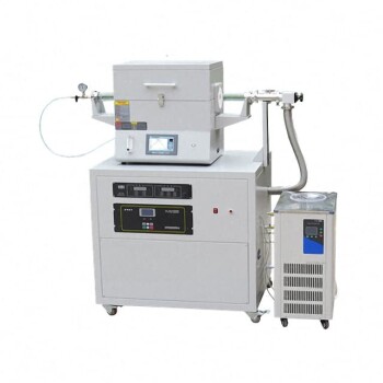
Split Chamber CVD Tube Furnace with Vacuum Station Chemical Vapor Deposition System Equipment Machine
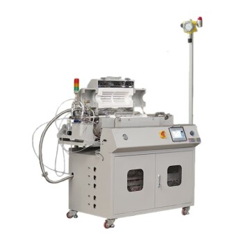
Customer Made Versatile CVD Tube Furnace Chemical Vapor Deposition Chamber System Equipment
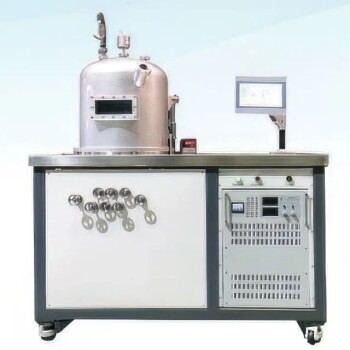
HFCVD Machine System Equipment for Drawing Die Nano-Diamond Coating
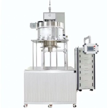
915MHz MPCVD Diamond Machine Microwave Plasma Chemical Vapor Deposition System Reactor
