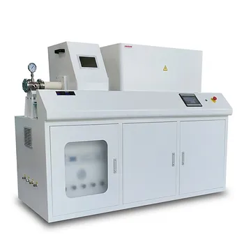
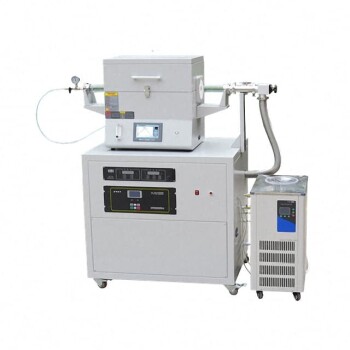
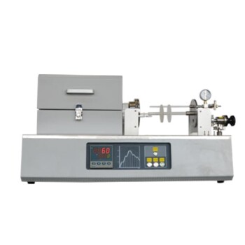
Thermal Chemical Vapor Deposition (CVD) is a deposition process where chemical reactions are driven specifically by thermal energy, supplied by heating either the substrate or the reaction chamber walls. In CMOS technology, this method is categorized into two primary sub-types based on operating pressure: Low-Pressure CVD (LPCVD) and Atmospheric Pressure CVD (APCVD).
Thermal CVD serves as the backbone of thin-film deposition in semiconductor manufacturing, leveraging heat to initiate chemical reactions. The choice between its two main sub-categories—LPCVD and APCVD—allows engineers to balance the need for high-precision film quality against cost and process complexity.
The Two Pillars of Thermal CVD in CMOS
Thermal CVD is the most common form of CVD used in CMOS technology. It is generally classified into two distinct categories based on the pressure environment within the reaction chamber.
Low-Pressure CVD (LPCVD)
LPCVD operates at reduced pressures to minimize gas-phase reactions and improve the mean free path of gas molecules.
This environment allows for significantly better process control and improved uniformity across the wafer.
It is typically utilized when depositing high-quality, conformal films, making it ideal for complex geometries where consistent coverage is critical.
Atmospheric Pressure CVD (APCVD)
APCVD operates at standard atmospheric pressure, eliminating the need for complex vacuum systems.
This process is generally simpler and more cost-effective to implement than low-pressure alternatives.
However, the trade-off is often lower film quality and uniformity compared to LPCVD, limiting its use to layers where extreme precision is less critical.
Why Thermal CVD is Essential
Despite the variations in pressure, the core thermal CVD process offers distinct advantages that make it indispensable for modern device fabrication.
Superior Conformality
CVD provides conformality, meaning it can coat complex surfaces evenly.
This is crucial for covering high-aspect-ratio features found in modern 3D structures and ensuring electrical continuity.
Material Versatility and Scalability
The process offers material versatility, capable of depositing a wide range of substances, including metals, dielectrics, and semiconductors.
Additionally, it offers scalability, making it suitable for cost-effective, large-scale production environments.
Excellent Uniformity
Thermal CVD ensures excellent uniformity, guaranteeing consistent physical and electrical properties across the entire device.
Understanding the Trade-offs
While Thermal CVD is powerful, it introduces specific engineering and safety challenges that must be managed.
Safety and Contamination Risks
The process often involves toxic, flammable, or reactive precursor gases, requiring rigorous safety protocols.
There is also a risk of potential contamination from residual byproducts, which can introduce defects and degrade device performance.
Process Complexity and Cost
Maintaining precise control over parameters like temperature, pressure, and precursor concentration is difficult, especially at scale.
Furthermore, the complexity of these systems leads to high equipment and operational costs, particularly when high-precision vacuum systems (LPCVD) are required.
Making the Right Choice for Your Goal
Selecting the appropriate Thermal CVD method requires analyzing the specific requirements of the layer being deposited.
- If your primary focus is high-performance and precision: Prioritize LPCVD to achieve superior uniformity and conformal coverage on complex topographies.
- If your primary focus is cost reduction and simplicity: Utilize APCVD for less critical layers where the highest degree of film quality is not mandatory.
Mastering Thermal CVD requires balancing the thermal energy required for reaction against the pressure controls necessary for film integrity.
Summary Table:
| Feature | Low-Pressure CVD (LPCVD) | Atmospheric Pressure CVD (APCVD) |
|---|---|---|
| Operating Pressure | Reduced/Low Pressure | Standard Atmospheric Pressure |
| Film Quality | High quality and superior uniformity | Generally lower quality/uniformity |
| Conformality | Excellent; ideal for complex 3D structures | Moderate; suited for simpler geometries |
| Process Complexity | High (requires vacuum systems) | Low (no vacuum required) |
| Primary Benefit | Precise control and consistency | Simplicity and cost-effectiveness |
Elevate your semiconductor manufacturing with KINTEK’s industry-leading deposition solutions. From high-performance thermal CVD systems and PECVD reactors to specialized consumables like crucibles and high-purity ceramics, we provide the tools necessary for superior material research and large-scale CMOS production. Whether you require precise LPCVD uniformity or cost-effective APCVD setups, our experts are ready to match you with the perfect high-temperature furnace or vacuum solution. Contact KINTEK today to enhance your lab's efficiency and film quality!
Related Products
- CVD Diamond for Thermal Management Applications
- Multi Heating Zones CVD Tube Furnace Machine Chemical Vapor Deposition Chamber System Equipment
- HFCVD Machine System Equipment for Drawing Die Nano-Diamond Coating
- Customer Made Versatile CVD Tube Furnace Chemical Vapor Deposition Chamber System Equipment
- Graphite Vacuum Furnace High Thermal Conductivity Film Graphitization Furnace
People Also Ask
- Are CVD diamonds real or fake? Discover the Truth About Lab-Grown Diamonds
- What is the hardness of CVD diamond? The Ultimate Guide to Engineered Super-Materials
- What is the chemical vapour deposition method for diamonds? Grow a Diamond from a Gas
- What are the characteristics of CVD diamond? Unlocking Superior Performance for Industrial Tools
- How do they make diamonds in CVD? Unlock the Secrets of Lab-Grown Diamond Creation
