Vapour Phase Epitaxy (VPE) is a crystal growth technique distinguished by its relatively simple equipment requirements and its capacity to produce high-purity materials with exceptional electrical properties. It is a foundational process in the semiconductor industry, widely utilized for manufacturing Silicon-based integrated circuits and high-performance Gallium Arsenide (GaAs) microwave devices.
VPE functions as a specialized form of Chemical Vapor Deposition (CVD) where gaseous chemicals grow a crystal layer that strictly maintains the substrate's orientation. Its balance of process simplicity and high-quality output makes it indispensable for creating both mass-market silicon chips and specialized microwave components like field-effect transistors.
The Defining Characteristics of VPE
VPE is defined by its ability to grow single-crystal thin layers using source chemicals in a gaseous state. It bridges the gap between ease of manufacturing and high-performance output.
Simplified Infrastructure
Unlike many competing epitaxial growth methods, VPE utilizes comparatively simple process equipment. This reduces operational complexity while maintaining high reliability in industrial environments.
Superior Material Purity
The process excels at growing materials with low contamination levels. It produces layers, particularly in Gallium Arsenide (GaAs), that exhibit excellent electrical properties essential for high-speed electronics.
Crystalline Continuity
VPE is fundamentally a type of Chemical Vapor Deposition (CVD). The grown thin layer is not merely a coating; it is a structural continuation of the single-crystal substrate, maintaining a corresponding relationship with the substrate's crystal orientation.
Primary Methodologies
While the core concept remains the same, the specific chemistry used in VPE varies based on the target material.
Silicon VPE Mechanisms
In Silicon VPE, high-purity hydrogen acts as both a transport and reduction gas. This reaction generates silicon atoms that deposit onto the substrate to form a single-crystal epitaxial layer.
GaAs VPE Techniques
For Gallium Arsenide growth, the industry typically employs two distinct approaches: the chloride method and the hydride method. These variations allow engineers to tailor the growth process to specific device requirements.
Industrial Applications
VPE is versatile, serving as a critical step in the production of both standard computing logic and high-frequency communication devices.
Silicon Semiconductor Production
VPE is a standard workhorse for the industrial production of silicon semiconductor devices. It is integral to the fabrication of the integrated circuits (ICs) that power most consumer electronics.
Microwave and Optoelectronic Devices
The technique is critical for producing GaAs-based components used in high-frequency applications. Specific implementations include:
- Hall devices
- Gunn diodes (referred to as Geng diodes in some contexts)
- Field-effect transistors (FETs)
Understanding the Trade-offs
Choosing the specific VPE method requires balancing the need for material purity against the specific application of the device.
Background Doping Levels
The chloride method is generally preferred for fabricating field-effect transistors. It yields layers with lower levels of background doping, which is crucial for minimizing noise in sensitive electronic signals.
Material Compatibility
Conversely, the hydride method is frequently selected for growing InGaAsP materials. This makes it the superior choice for manufacturing laser devices, whereas the chloride method is less suited for this specific compound.
Making the Right Choice for Your Goal
Selecting the correct VPE application depends entirely on whether you are prioritizing mass logic fabrication or specialized high-frequency performance.
- If your primary focus is Silicon fabrication: Rely on VPE using hydrogen transport to create standard integrated circuits with high structural integrity.
- If your primary focus is low-noise transistors: Utilize the chloride method of GaAs VPE to minimize background doping and ensure superior electrical performance.
- If your primary focus is laser devices: Opt for the hydride method to effectively grow InGaAsP materials suited for optoelectronics.
By selecting the specific VPE methodology that aligns with your material requirements, you can achieve the precise crystal structure necessary for high-performance semiconductor devices.
Summary Table:
| Feature | Chloride Method (GaAs) | Hydride Method (GaAs) | Silicon VPE |
|---|---|---|---|
| Primary Use | Low-noise transistors (FETs) | Laser devices (InGaAsP) | Integrated Circuits (ICs) |
| Key Advantage | Lower background doping | Material compatibility | High structural integrity |
| Process Gas | Chloride-based chemistry | Hydride-based chemistry | Hydrogen (Transport/Reduction) |
| Output | High-performance microwave | Optoelectronics | Mass-market logic chips |
Elevate Your Semiconductor Research with KINTEK
Precision in crystal growth requires exceptional thermal control and high-purity environments. KINTEK specializes in advanced laboratory equipment, including CVD systems, high-temperature furnaces (muffle, tube, and vacuum), and high-purity ceramics and crucibles essential for Vapour Phase Epitaxy.
Whether you are developing high-speed GaAs microwave devices or next-generation silicon integrated circuits, our comprehensive range of high-performance reactors, cooling solutions, and specialized consumables ensures your lab achieves superior material purity and electrical properties.
Ready to optimize your epitaxial growth process? Contact KINTEK today for expert consultation and tailored laboratory solutions!
Related Products
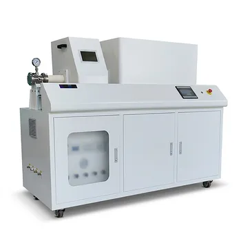
- Inclined Rotary Plasma Enhanced Chemical Vapor Deposition PECVD Equipment Tube Furnace Machine
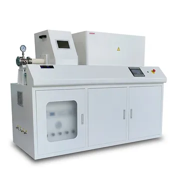
- Chemical Vapor Deposition CVD Equipment System Chamber Slide PECVD Tube Furnace with Liquid Gasifier PECVD Machine
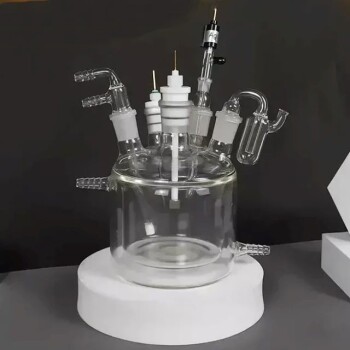
- Double Layer Five-Port Water Bath Electrolytic Electrochemical Cell
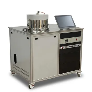
- RF PECVD System Radio Frequency Plasma-Enhanced Chemical Vapor Deposition RF PECVD
- Inclined Rotary Plasma Enhanced Chemical Vapor Deposition PECVD Equipment Tube Furnace Machine
People Also Ask
- What is plasma enhanced chemical vapor deposition PECVD equipment? A Guide to Low-Temperature Thin Film Deposition
- What are the advantages of plasma enhanced chemical vapor deposition? Enable Low-Temperature, High-Quality Film Deposition
- How does PECVD equipment facilitate the directional growth of carbon nanotubes? Achieve Precision Vertical Alignment
- What is the process of PECVD in semiconductor? Enabling Low-Temperature Thin Film Deposition
- How does PECVD process work? Achieve Low-Temperature, High-Quality Thin Films
