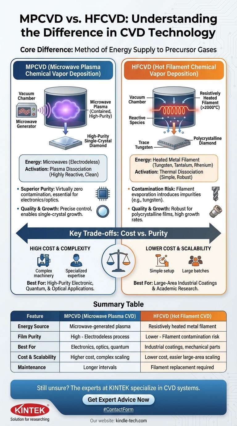
At its core, the difference between MPCVD (Microwave Plasma Chemical Vapor Deposition) and HFCVD (Hot Filament Chemical Vapor Deposition) is the method used to supply energy to the precursor gases. MPCVD uses microwaves to generate a contained, high-purity plasma, while HFCVD uses a resistively heated metal wire (a filament) to thermally break down the gases. This fundamental distinction in energy sources dictates the purity, cost, and scalability of each process.
The central decision between MPCVD and HFCVD is a trade-off between film purity and operational cost. MPCVD provides superior purity essential for electronics and optics, whereas HFCVD offers a simpler, more scalable, and cost-effective solution for industrial coatings where minor contamination is acceptable.

The Fundamental Difference: Activating the Gas
Both methods fall under the umbrella of Chemical Vapor Deposition (CVD), a process where gases react to form a solid film on a substrate. The key is how you "activate" those gases into a reactive state.
MPCVD: The Power of Microwave Plasma
In Microwave Plasma CVD, microwaves (typically at 2.45 GHz) are channeled into a vacuum chamber. This energy ignites the precursor gases (like methane and hydrogen for diamond growth) into a plasma, an ionized state of matter.
This plasma is a highly energetic and reactive environment. The energetic electrons and ions efficiently dissociate the gas molecules, creating the chemical species needed for film growth on the substrate. The process is electrodeless, meaning the energy is coupled into the gas remotely, which is critical for purity.
HFCVD: The Simplicity of Thermal Activation
In Hot Filament CVD, a refractory metal wire—often made of tungsten, tantalum, or rhenium—is positioned a few centimeters above the substrate. This filament is heated to extreme temperatures, typically above 2000°C.
As the precursor gases flow over this intensely hot wire, they are thermally dissociated. The molecules break apart due to the heat, creating the necessary reactive species. This method relies on simple thermal energy rather than complex plasma physics.
Key Performance and Process Implications
The choice of energy source has direct consequences on the final product and the process itself.
Film Purity and Contamination
This is the most significant differentiator. MPCVD is an inherently cleaner process. Because the plasma is generated without direct contact with electrodes, the risk of contamination from the energy source is virtually zero. This makes it the standard for high-purity materials like electronic-grade or gem-grade diamond.
HFCVD is prone to contamination. The hot filament inevitably evaporates or sputters over time, introducing trace amounts of the filament material (e.g., tungsten) into the growing film. While often negligible for mechanical applications, this contamination is unacceptable for high-performance electronic or optical components.
Growth Rate and Quality
Both methods can achieve high-quality film growth. MPCVD allows for precise control over plasma density and ion energy, enabling the growth of high-quality single-crystal diamond under specific conditions.
HFCVD is a robust method for growing high-quality polycrystalline diamond films. Growth rates are generally high and easily controlled by adjusting gas flow and filament temperature.
Scalability and Uniformity
HFCVD is generally easier and cheaper to scale for large-area deposition. One can simply design larger filament arrays to cover bigger substrates uniformly. This makes it a workhorse for coating large batches of industrial parts, like cutting tools or wear surfaces.
Scaling MPCVD can be more complex, as maintaining a uniform, stable plasma over a very large area presents significant engineering challenges. However, modern systems achieve excellent uniformity over substrates several inches in diameter.
Understanding the Trade-offs: Cost vs. Purity
Choosing between these two technologies is an exercise in balancing performance requirements with economic reality.
The High Cost of Purity (MPCVD)
MPCVD systems are more complex and expensive. They require a microwave generator, waveguides, impedance matching systems, and a carefully designed reactor chamber. The operational expertise required is also higher. This cost is justified when the absolute highest purity is non-negotiable.
The Contamination Risk of Simplicity (HFCVD)
HFCVD systems are mechanically simple, significantly cheaper to build, and easier to operate and maintain. This accessibility makes them highly popular in university research labs and for industrial applications where the primary concern is mechanical properties (like hardness) rather than electronic properties. The trade-off is the accepted, low-level contamination.
System Complexity and Maintenance
Filaments in an HFCVD system are a consumable part. They degrade over time, especially in the presence of certain gases, and require periodic replacement. MPCVD systems, lacking this consumable component in the chamber, generally offer longer maintenance intervals related to the core process.
Making the Right Choice for Your Application
Your final decision must be guided by the specific requirements of your end product.
- If your primary focus is high-purity electronic, quantum, or optical applications: MPCVD is the only viable choice due to its inherently clean, electrodeless process.
- If your primary focus is large-area industrial coatings (e.g., tools, wear parts): HFCVD provides a superior balance of performance, scalability, and cost-effectiveness.
- If you are in academic research with a limited budget: HFCVD offers a more accessible and simpler entry point for studying fundamental film growth and material properties.
Ultimately, you are choosing the right tool for the job by matching the process characteristics to your material's performance targets.
Summary Table:
| Feature | MPCVD (Microwave Plasma CVD) | HFCVD (Hot Filament CVD) |
|---|---|---|
| Energy Source | Microwave-generated plasma | Resistively heated metal filament |
| Film Purity | High (electrodeless process) | Lower (filament contamination risk) |
| Best For | Electronics, optics, quantum applications | Industrial coatings, mechanical parts |
| Cost & Scalability | Higher cost, complex scaling | Lower cost, easier large-area scaling |
| Maintenance | Longer intervals (no consumable filament) | Filament replacement required |
Still unsure which CVD method is right for your project? The experts at KINTEK are here to help. We specialize in lab equipment and consumables for all your laboratory needs, including CVD systems for both research and industrial applications.
Our team can provide personalized guidance to match your specific requirements for purity, scalability, and budget. Contact us today for a consultation and let us help you achieve optimal results with the right technology.
Visual Guide
Related Products
- 915MHz MPCVD Diamond Machine Microwave Plasma Chemical Vapor Deposition System Reactor
- Cylindrical Resonator MPCVD Machine System Reactor for Microwave Plasma Chemical Vapor Deposition and Lab Diamond Growth
- Microwave Plasma Chemical Vapor Deposition MPCVD Machine System Reactor for Lab and Diamond Growth
- Multi Heating Zones CVD Tube Furnace Machine Chemical Vapor Deposition Chamber System Equipment
- Inclined Rotary Plasma Enhanced Chemical Vapor Deposition PECVD Equipment Tube Furnace Machine
People Also Ask
- Why is MW-CVD preferred for high-purity diamond optical windows? Achieve Zero-Contamination Material Growth
- What are the advantages of a Microwave Plasma CVD reactor for MCD/NCD coatings? Precision Multilayer Diamond Engineering
- How does a microwave plasma reactor facilitate the synthesis of diamond? Master MPCVD with Precision Technology
- What pressure is needed for chemical vapor deposition of diamonds? Master the Low-Pressure 'Sweet Spot'
- How are CVD diamonds created? Discover the Science of Lab-Grown Diamond Precision


