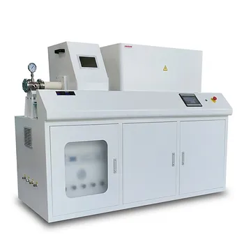
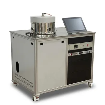
MOCVD (Metal Organic Chemical Vapor Deposition) is the premier technology for manufacturing complex semiconductor devices, prized for its ability to balance atomic-level precision with the demands of large-scale industrial production. Its primary advantage lies in the precise control of gas flow rates, which allows for the growth of high-purity, ultra-thin epitaxial layers essential for advanced microelectronics and optoelectronics.
MOCVD serves as a bridge between laboratory precision and factory throughput, enabling the creation of steep material interfaces and uniform heterostructures without the extreme vacuum requirements of competing technologies.
Precision and Process Control
Precise Layer Definition
MOCVD offers exceptional control over the thickness, composition, and dopant concentration of the epitaxial layer. By strictly managing gas flow rates and reaction times, engineers can grow thin and ultra-thin layers with exacting specifications.
Linear Growth Adjustability
The growth rate in an MOCVD reactor is directly proportional to the flow rate of the Group III source material. This linear relationship allows for wide and predictable adjustability during the fabrication process.
In-Situ Monitoring capabilities
Modern MOCVD systems utilize advanced detection technology to monitor the growth process in real-time. This ensures immediate feedback and quality control without interrupting the deposition cycle.
Superior Interface Quality for Advanced Devices
Rapid Composition Switching
The technology utilizes fast gas flow rates, which facilitates quick changes in material composition within the reactor. This speed is critical for reducing "memory effects," where residual gases contaminate the next layer.
Steep Interfaces for Quantum Structures
Because gas compositions can change rapidly, MOCVD creates very steep interfaces between different material layers. This capability is vital for fabricating high-performance heterostructures and quantum wells used in lasers and LEDs.
Industrial Scalability and Flexibility
Large-Scale Homogeneity
MOCVD relies on a single-temperature pyrolytic reaction combined with uniform airflow. This thermal and aerodynamic stability ensures excellent uniformity across large areas, making it highly suitable for mass production.
Extensive Material Versatility
The system is incredibly flexible regarding the materials it can produce. By selecting the appropriate organometallic raw materials, manufacturers can grow almost all types of compound and alloy semiconductors.
Simplified Infrastructure
Compared to other high-precision deposition methods, MOCVD has lower vacuum requirements. This simplifies the structure of the reaction chamber and reduces the complexity of the supporting infrastructure.
Understanding the Trade-offs
Precursor Cost and Safety Hazards
The primary downside of MOCVD lies in the reaction sources; the metal-organic compounds and hydrides required are often expensive. Furthermore, many of these sources are flammable, explosive, or toxic, necessitating strict safety protocols and waste treatment to prevent environmental contamination.
Risk of Unintentional Doping
Because the precursor sources contain elements like Carbon (C) and Hydrogen (H), there is a risk of introducing these elements as impurities into the film. The reaction process requires careful thermal control to minimize this unintentional doping.
Making the Right Choice for Your Goal
While MOCVD is a dominant technology, its application depends on your specific manufacturing priorities.
- If your primary focus is Mass Production: Leverage MOCVD for its ability to maintain high uniformity and throughput across large wafer areas.
- If your primary focus is Complex Device Architecture: Utilize MOCVD to achieve the steep interfaces required for quantum wells and heterostructure devices.
- If your primary focus is Cost Minimization: Be aware that high precursor costs and safety infrastructure requirements may impact the initial return on investment.
MOCVD remains the definitive choice for manufacturers who require a scalable solution for growing high-quality, complex compound semiconductors.
Summary Table:
| Feature | Advantage | Industrial Impact |
|---|---|---|
| Layer Control | Atomic-level thickness & doping precision | High-performance microelectronics |
| Interface Quality | Steep interfaces & rapid switching | Optimized quantum wells & LEDs |
| Scalability | High uniformity across large areas | Efficient mass production |
| Flexibility | Wide range of compounds & alloys | Versatile device fabrication |
| Infrastructure | Lower vacuum requirements | Simplified chamber design |
Elevate Your Semiconductor Fabrication with KINTEK
Unlock the full potential of MOCVD technology with KINTEK’s industry-leading expertise. Whether you are developing high-performance lasers, LEDs, or complex heterostructures, KINTEK provides the specialized equipment and consumables needed for success.
Our extensive portfolio includes precision high-temperature furnaces (CVD, PECVD, MPCVD, and vacuum), cutting-edge high-pressure reactors, and a complete range of laboratory tools from hydraulic presses to PTFE consumables and ceramics. We empower target customers—from researchers to industrial manufacturers—with reliable, high-purity solutions that bridge the gap between laboratory innovation and large-scale throughput.
Ready to optimize your epitaxial growth? Contact our technical experts today to discuss how our solutions can enhance your lab's efficiency and product quality.
Related Products
- Multi Heating Zones CVD Tube Furnace Machine Chemical Vapor Deposition Chamber System Equipment
- 915MHz MPCVD Diamond Machine Microwave Plasma Chemical Vapor Deposition System Reactor
- Microwave Plasma Chemical Vapor Deposition MPCVD Machine System Reactor for Lab and Diamond Growth
- Cylindrical Resonator MPCVD Machine System Reactor for Microwave Plasma Chemical Vapor Deposition and Lab Diamond Growth
- Molybdenum Vacuum Heat Treat Furnace
People Also Ask
- What is the function of a tube furnace in CVD SiC synthesis? Achieving Ultra-Pure Silicon Carbide Powders
- How does a CVD tube furnace inhibit the sintering of silver supports? Boost Membrane Durability and Performance
- What is a CVD tube furnace? A Complete Guide to Thin-Film Deposition
- What advantages do CVD furnaces offer for Wf/W composites? Preserving Fiber Ductility and Interface Integrity
- What is the function of a high-temperature CVD tube furnace in 3D graphene foam prep? Master 3D Nanomaterial Growth

