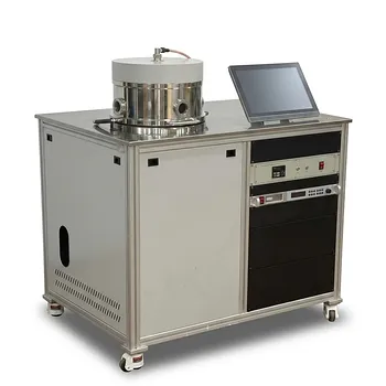
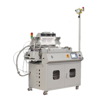
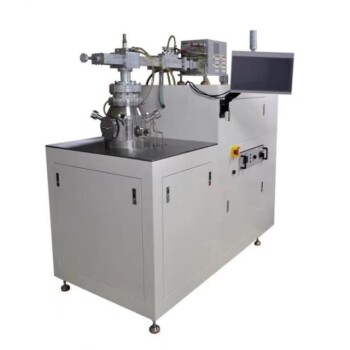
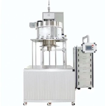
High-Density Plasma Chemical Vapour Deposition (HDPCVD) is an advanced thin-film deposition technique that utilizes an inductively coupled plasma (ICP) source to generate superior film quality at low temperatures. Unlike conventional Plasma Enhanced Chemical Vapour Deposition (PECVD), HDPCVD separates the control of ion flux from ion energy, allowing for precise manipulation of the deposition process. This method is specifically engineered to fill microscopic gaps and trenches in semiconductor manufacturing without creating voids.
Core Takeaway HDPCVD is the industry solution for "gap-fill" challenges in modern microelectronics. By combining simultaneous deposition and etching within the same chamber, it can fill high-aspect-ratio trenches (smaller than 0.8 microns) that standard methods would block off, making it essential for applications like CMOS Shallow Trench Isolation (STI).
The Core Mechanism: Inductively Coupled Plasma
HDPCVD differs from standard methods primarily through its plasma source. While traditional systems often use capacitive coupling, HDPCVD employs an Inductively Coupled Plasma (ICP) source.
High Density at Low Temperatures
The ICP source generates a significantly higher density of ions compared to traditional PECVD. This allows the process to occur at lower deposition temperatures while maintaining high film quality.
Independent Process Control
A defining feature of this technology is the ability to control ion flux (the quantity of ions) independently from ion energy (how hard they hit the surface). In standard systems, these parameters are often coupled, limiting process flexibility. Decoupling them allows engineers to fine-tune the impact of the plasma on the wafer surface.
Key Features and Capabilities
Simultaneous Deposition and Etching
The most critical innovation of HDPCVD is that deposition and etching occur at the same time. As the chemical vapor deposits material onto the wafer, the high-density plasma simultaneously creates a sputtering (etching) effect.
This is vital for filling deep trenches. The sputtering effect prevents material from accumulating too quickly at the "mouth" of a trench, keeping the opening wide enough for material to reach and fill the bottom. This capability allows HDPCVD to effectively fill high-aspect-ratio gaps smaller than 0.8 microns without trapping air pockets (voids).
Superior Film Quality
Films produced via HDPCVD exhibit excellent characteristics compared to standard methods. The process improves film densification and ensures the growth of high-quality material even at temperatures far below the melting point of the substrate. This results in films with low residual stress and high purity.
Application in CMOS Manufacturing
Due to its gap-filling prowess, HDPCVD is the standard method for Shallow Trench Isolation (STI) in CMOS integrated circuits. It ensures the electrical isolation structures between transistors are solid and reliable.
Operational Advantages and Trade-offs
Hardware Versatility (The "2-in-1" Advantage)
A significant operational benefit is hardware flexibility. An HDPCVD system can often be converted into an Inductively Coupled Plasma-Reactive Ion Etching (ICP-RIE) system.
This implies that the same core machinery can perform both deposition and dedicated etching tasks (with reconfiguration). This is highly beneficial for facilities with limited budgets or restricted cleanroom footprint, as it reduces the need for two completely separate tool sets.
Understanding the Context
While powerful, HDPCVD is a specialized tool.
- Complexity: The simultaneous dep/etch process requires careful balancing of parameters (chemical composition, morphology, grain size) to ensure the trench fills rather than erodes.
- Throughput vs. Quality: The etching component of the process naturally competes with the deposition rate. While it ensures a void-free fill, it is a more complex dynamic than simple "blanket" deposition methods used for flat surfaces.
Making the Right Choice for Your Goal
HDPCVD is not a replacement for all CVD processes, but a specific solution for complex geometries and resource constraints.
- If your primary focus is Void-Free Gap Fill: Choose HDPCVD for its simultaneous deposition and etching capability, which is essential for filling trenches <0.8 microns in CMOS/STI applications.
- If your primary focus is Film Density at Low Temp: Leverage the ICP source to produce dense, high-quality films without subjecting the substrate to the high thermal stress of traditional high-temperature CVD.
- If your primary focus is Budget or Footprint: Utilize the system's convertibility to ICP-RIE, allowing a single tool platform to handle both deposition and etching steps at different times.
HDPCVD represents the optimal balance of physical impact and chemical reaction, ensuring structural integrity in the smallest features of modern electronics.
Summary Table:
| Feature | HDPCVD Specification | Advantage |
|---|---|---|
| Plasma Source | Inductively Coupled Plasma (ICP) | High ion density at lower process temperatures |
| Gap-Fill Capability | < 0.8 microns | Prevents voids in high-aspect-ratio trenches |
| Process Dynamic | Simultaneous Deposition & Etching | Keeps trench openings clear for complete filling |
| Control Mechanism | Independent Flux & Energy Control | Precise manipulation of film quality and stress |
| Versatility | Convertible to ICP-RIE | Dual-use hardware for deposition and etching |
Precision Thin-Film Solutions for Your Laboratory
At KINTEK, we understand that achieving void-free gap fill and superior film density is critical for advanced semiconductor research. Our specialized range of CVD, PECVD, and HDPCVD systems is designed to meet the rigorous demands of modern microelectronics.
Beyond deposition, KINTEK offers a comprehensive portfolio including:
- High-Temperature Furnaces: Muffle, tube, and vacuum systems for thermal processing.
- Sample Preparation: Crushing, milling, sieving, and hydraulic presses (pellet, hot, isostatic).
- Specialized Reactors: High-temperature high-pressure reactors and autoclaves.
- Electrochemical Tools: Advanced electrolytic cells and electrodes.
- Lab Essentials: ULT freezers, homogenizers, and high-purity ceramics/PTFE consumables.
Whether you are optimizing CMOS manufacturing or developing new battery technologies, our experts are ready to provide the high-performance tools you need. Contact KINTEK today to discuss your project requirements!
Related Products
- HFCVD Machine System Equipment for Drawing Die Nano-Diamond Coating
- Chemical Vapor Deposition CVD Equipment System Chamber Slide PECVD Tube Furnace with Liquid Gasifier PECVD Machine
- RF PECVD System Radio Frequency Plasma-Enhanced Chemical Vapor Deposition RF PECVD
- Inclined Rotary Plasma Enhanced Chemical Vapor Deposition PECVD Equipment Tube Furnace Machine
- Microwave Plasma Chemical Vapor Deposition MPCVD Machine System Reactor for Lab and Diamond Growth
People Also Ask
- What are the disadvantages and challenges of the HFCVD method? Overcome Growth Limits and Filament Issues
- Why is Chemical Vapor Deposition (CVD) equipment uniquely suited for constructing hierarchical superhydrophobic structures?
- What is the function of tungsten filaments in HFCVD? Powering Diamond Film Synthesis with Thermal Excitation
- What is the full form of HFCVD? A Guide to Hot Filament Chemical Vapor Deposition
- What types of substrates are used in CVD to facilitate graphene films? Optimize Graphene Growth with the Right Catalyst
