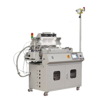
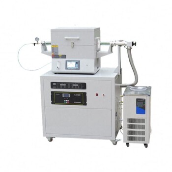
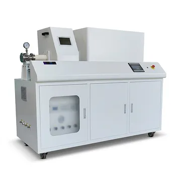
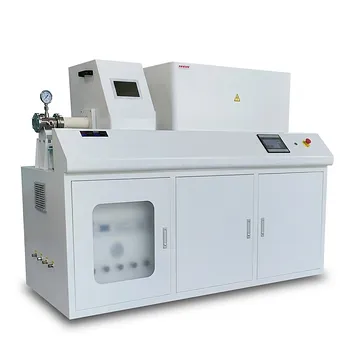
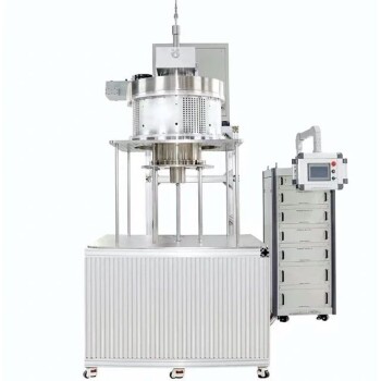
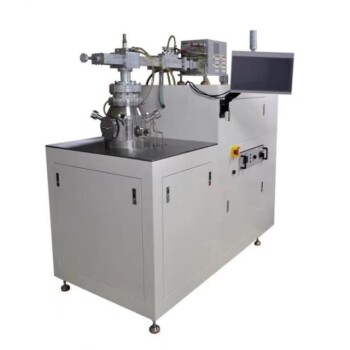
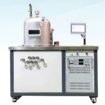
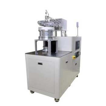
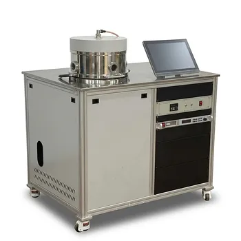
ICPCVD systems are primarily characterized by their ability to deposit high-quality, low-damage films while maintaining exceptionally low substrate temperatures. These systems provide a versatile processing environment capable of handling temperatures as low as 5°C, making them ideal for temperature-sensitive substrates while supporting standard dielectric and semiconductor material deposition.
The core value of an ICPCVD system lies in decoupling plasma density from ion energy, allowing for the deposition of high-quality films like SiO2 and SiC on wafers up to 200mm without the thermal damage associated with conventional high-temperature processes.
Thermal Versatility and Substrate Protection
Ultra-Low Temperature Processing
One of the most distinct capabilities of these systems is the ability to maintain substrate temperatures as low as 5°C. This allows for processing on delicate substrates that cannot withstand standard thermal budgets.
Broad Electrode Temperature Range
The system offers significant thermal flexibility, with an electrode temperature range spanning from 5°C up to 400°C. This wide window allows engineers to tune film properties by adjusting thermal energy without locking the process into a high-heat regime.
Material Versatility and Film Quality
High-Quality Dielectrics and Semiconductors
The system is optimized to deposit a variety of essential fabrication materials. Standard process capabilities include Silicon Dioxide (SiO2), Silicon Nitride (Si3N4), and Silicon Oxynitride (SiON).
Advanced Material Support
Beyond standard dielectrics, the system supports the deposition of Silicon (Si) and Silicon Carbide (SiC). The resulting films are noted for being high-quality and exhibiting low damage, a critical factor for high-performance device layers.
Process Scalability and Control
Wafer Size Accommodation
These systems are designed to scale effectively for research and mid-volume production. They accommodate wafer sizes up to 200mm, covering the vast majority of specialized semiconductor and MEMS applications.
Optimizing Uniformity via Source Sizing
To ensure process uniformity across different wafer sizes, the Inductively Coupled Plasma (ICP) source is modular. It is available in three distinct sizes: 65mm, 180mm, and 300mm.
Operational Efficiency
Integrated Chamber Cleaning
To maintain process repeatability and reduce particle contamination, the system supports in-situ chamber cleaning.
Precision Endpoint Monitoring
The cleaning process is governed by real-time endpoint monitoring. This prevents over-etching of chamber components and ensures the system is returned to a pristine state efficiently between runs.
Understanding Operational Considerations
Matching Source Size to Application
While the system supports wafers up to 200mm, uniformity is heavily dependent on hardware configuration. You must ensure the selected ICP source size (65mm, 180mm, or 300mm) creates a plasma field strictly appropriate for your specific substrate dimensions to avoid edge effects.
Thermal Trade-offs
While the system is capable of 400°C operation, its defining feature is the low-temperature capability (5°C). Users operating exclusively at the high end of this range (400°C) should verify that the specific hardware configuration and cooling loops are optimized for sustained high-temp throughput.
Making the Right Choice for Your Goal
When evaluating an ICPCVD system for your fabrication line, consider your specific processing priorities:
- If your primary focus is Temperature-Sensitive Substrates: Leverage the system's ability to hold substrates at 5°C to deposit films without thermal degradation.
- If your primary focus is Process Uniformity: Select the ICP source size (up to 300mm) that provides the optimal coverage for your specific wafer diameter (up to 200mm).
- If your primary focus is Film Integrity: Rely on the system's low-damage deposition capabilities for critical layers involving SiO2, Si3N4, or SiC.
This system effectively bridges the gap between high-quality film requirements and strict thermal constraints.
Summary Table:
| Feature | Specification / Capability |
|---|---|
| Temperature Range | 5°C to 400°C |
| Wafer Size Support | Up to 200 mm |
| Standard Materials | SiO2, Si3N4, SiON |
| Advanced Materials | Silicon (Si), Silicon Carbide (SiC) |
| ICP Source Sizes | 65mm, 180mm, 300mm |
| Key Features | In-situ cleaning & Real-time endpoint monitoring |
Elevate Your Semiconductor Fabrication with KINTEK
Are you working with temperature-sensitive substrates or requiring high-integrity dielectric films? KINTEK specializes in advanced laboratory solutions, offering cutting-edge ICPCVD systems and a comprehensive range of high-temperature furnaces, vacuum systems, and PECVD tools tailored for precise material research.
Our expertise extends across laboratory equipment and consumables—from high-temperature reactors to PTFE and ceramic crucibles—ensuring your lab has the reliability and precision needed for breakthrough results.
Ready to optimize your deposition process? Contact our technical specialists today to find the perfect equipment configuration for your research goals.
Related Products
- Customer Made Versatile CVD Tube Furnace Chemical Vapor Deposition Chamber System Equipment
- Split Chamber CVD Tube Furnace with Vacuum Station Chemical Vapor Deposition System Equipment Machine
- Inclined Rotary Plasma Enhanced Chemical Vapor Deposition PECVD Equipment Tube Furnace Machine
- Chemical Vapor Deposition CVD Equipment System Chamber Slide PECVD Tube Furnace with Liquid Gasifier PECVD Machine
- 915MHz MPCVD Diamond Machine Microwave Plasma Chemical Vapor Deposition System Reactor
People Also Ask
- What is the function of a tube furnace in CVD SiC synthesis? Achieving Ultra-Pure Silicon Carbide Powders
- What is the difference between hot wall CVD and cold wall CVD? Choose the Right System for Your Process
- What is the function of a high-temperature CVD tube furnace in 3D graphene foam prep? Master 3D Nanomaterial Growth
- What is the synthesis and mechanism involved in the preparation of carbon nanotubes using CVD process? Master Controlled Growth for Your Application
- How does a CVD tube furnace inhibit the sintering of silver supports? Boost Membrane Durability and Performance
