Low Pressure Chemical Vapour Deposition (LPCVD) is a specialized thermal process used primarily in the semiconductor industry to deposit high-quality thin films with exceptional precision. Its main advantages include superior film uniformity, precise resistivity control, and excellent "step coverage," allowing it to effectively coat complex geometries and deep trenches. Furthermore, because it operates without carrier gases, LPCVD minimizes particle contamination and allows for high-volume batch processing of materials ranging from silicon nitride to graphene.
The core value of LPCVD lies in its ability to trade atmospheric pressure for precision and purity. By operating in a low-pressure, high-temperature environment, it extends the mean free path of gas molecules, enabling uniform coating of densely packed wafers without the interference of carrier gas contaminants.
The Technical Advantages of LPCVD
Superior Uniformity and Step Coverage
LPCVD operates at reduced pressures, typically below 133 Pa. This low-pressure environment significantly increases the gas diffusion coefficient and the "mean free path" (the distance a molecule travels before colliding with another).
Consequently, the gas can penetrate deep into trenches and complex structures before reacting. This results in films with high conformality, ensuring that vertical walls and bottoms of trenches are coated as evenly as flat surfaces.
High Purity and Reduced Contamination
Unlike Atmospheric Pressure CVD (APCVD), LPCVD does not require a carrier gas to transport the chemical vapor. Eliminating carrier gases removes a significant source of particle pollution, leading to cleaner films.
Additionally, the process facilitates the rapid transport and removal of impurities and reaction by-products. This efficiency suppresses "self-doping" (unwanted incorporation of impurities), ensuring the deposited film maintains precise chemical composition and resistivity.
High-Throughput Batch Processing
The enhanced mass transfer rates inherent to LPCVD allow for a unique loading configuration. Wafers can be loaded vertically and packed closely together without sacrificing coating quality.
This capability creates a massive advantage in production efficiency. While the deposition rate on a single wafer might be moderate, the ability to process a large number of wafers simultaneously in a single batch results in high overall output.
Key Applications and Materials
Semiconductor Insulators and Conductors
LPCVD is the industry standard for preparing essential layers in integrated circuits. It is extensively used to deposit polycrystalline silicon (doped and undoped), which serves as gate electrodes and interconnects.
It is also the method of choice for dielectric films such as silicon dioxide and silicon nitride. Furthermore, it is used to create specialized glasses like phosphor-silica glass (PSG) and boron-phosphor-silica glass (BPSG), which are critical for planarization and insulation.
Advanced Nanomaterials
Beyond standard semiconductor films, LPCVD is utilized in the production of cutting-edge nanotechnology. It is an effective method for synthesizing graphene and carbon nanotubes.
These materials require the high structural control and purity that the low-pressure environment provides, making LPCVD vital for next-generation electronics and material science research.
Understanding the Trade-offs
Thermal Budget Constraints
The LPCVD process generally operates in a "high thermal environment." While this improves film density and quality, it imposes a thermal budget constraint on the manufacturing flow.
You must ensure that the substrate and any previously deposited layers can withstand these elevated temperatures without degrading or diffusing unwantedly.
Complexity vs. Speed
While the batch output is high, the deposition rate per minute can be lower compared to other methods like APCVD. The process relies on strict vacuum maintenance and temperature control, which can increase the complexity of the equipment compared to non-vacuum techniques.
Making the Right Choice for Your Goal
- If your primary focus is Geometric Precision: Choose LPCVD for its superior step coverage, which is essential for filling deep trenches and coating complex 3D structures.
- If your primary focus is Film Purity: Rely on LPCVD to minimize particle contamination and auto-doping by eliminating the need for carrier gases.
- If your primary focus is Production Volume: Leverage the vertical, close-packed wafer loading capability to maximize the number of units processed per batch.
LPCVD remains the definitive choice when the quality, uniformity, and purity of the film are more critical than low-temperature processing.
Summary Table:
| Feature | LPCVD Advantage | Key Benefit |
|---|---|---|
| Film Uniformity | High Mean Free Path | Exceptional step coverage for deep trenches and 3D structures. |
| Purity Level | No Carrier Gas Required | Minimizes particle contamination and prevents unwanted self-doping. |
| Production Rate | Close-Packed Batch Processing | High-volume throughput by processing many wafers simultaneously. |
| Materials | Diverse Synthesis | Ideal for Polysilicon, Silicon Nitride, Graphene, and Nanotubes. |
Elevate Your Thin-Film Precision with KINTEK
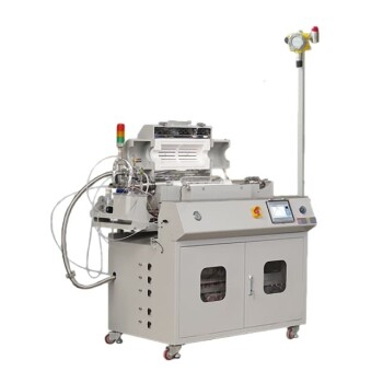
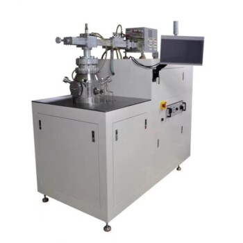
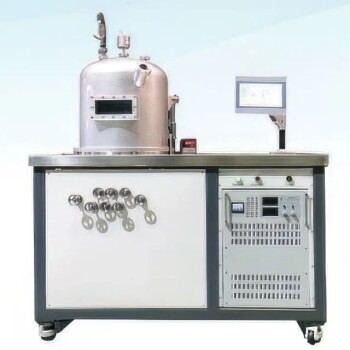
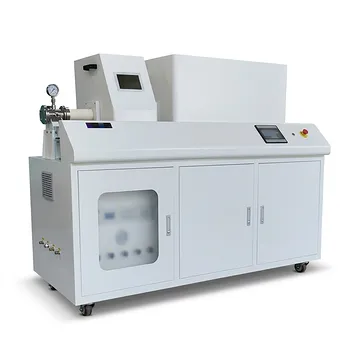
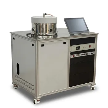
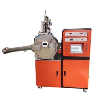
Ready to achieve unmatched film purity and uniformity in your lab or production line? KINTEK specializes in high-performance laboratory equipment, providing advanced LPCVD systems, high-temperature vacuum furnaces, and CVD/PECVD solutions tailored for the semiconductor and nanotechnology industries.
Whether you are synthesizing graphene or depositing critical dielectric layers, our comprehensive portfolio—including high-temperature high-pressure reactors, ceramic crucibles, and cooling solutions—ensures your research meets the highest standards.
Maximize your batch efficiency today. Contact our technical experts at KINTEK to find your perfect solution!
Related Products
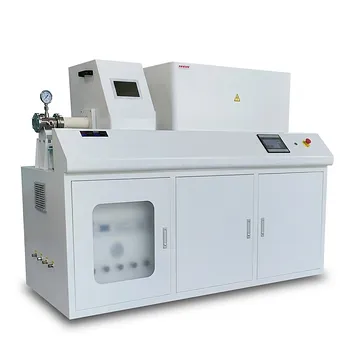
- Chemical Vapor Deposition CVD Equipment System Chamber Slide PECVD Tube Furnace with Liquid Gasifier PECVD Machine
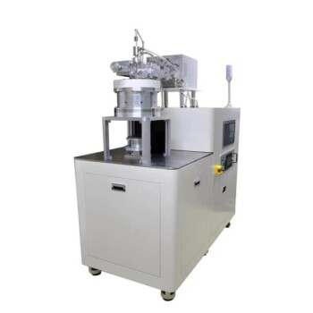
- Microwave Plasma Chemical Vapor Deposition MPCVD Machine System Reactor for Lab and Diamond Growth
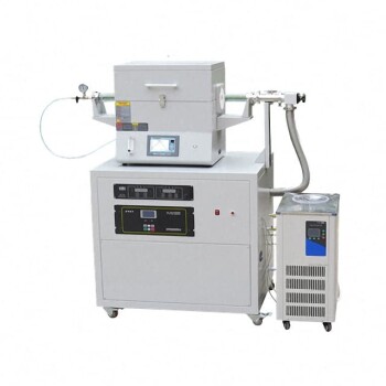
- Split Chamber CVD Tube Furnace with Vacuum Station Chemical Vapor Deposition System Equipment Machine
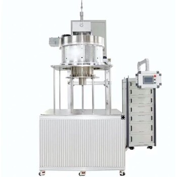
- 915MHz MPCVD Diamond Machine Microwave Plasma Chemical Vapor Deposition System Reactor
- Customer Made Versatile CVD Tube Furnace Chemical Vapor Deposition Chamber System Equipment
People Also Ask
- What is plasma enhanced chemical vapor deposition PECVD equipment? A Guide to Low-Temperature Thin Film Deposition
- What are the core advantages of PE-CVD in OLED encapsulation? Protect Sensitive Layers with Low-Temp Film Deposition
- How expensive is chemical vapor deposition? Understanding the True Cost of High-Performance Coating
- What happens during deposition chemistry? Building Thin Films from Gaseous Precursors
- What types of substrates are used in CVD to facilitate graphene films? Optimize Graphene Growth with the Right Catalyst
