The primary application of High-Density Plasma Chemical Vapor Deposition (HDP-CVD) is the precise filling of microscopic dielectric gaps during the fabrication of semiconductor devices. It is specifically engineered to handle the demanding geometries of Shallow Trench Isolation (STI) and dielectric interlayers for technology nodes ranging from 180 nm down to 45 nm.
Core Takeaway: While standard CVD is used broadly for surface coatings, HDP-CVD is a specialized process essential for the structural integrity of modern microchips. Its main function is to deposit insulating material into extremely small, deep gaps between transistors without leaving voids.
The Role of HDP-CVD in Semiconductor Manufacturing
The semiconductor industry relies on HDP-CVD to solve specific geometric challenges that arise as devices shrink. Unlike general coating processes, this technology focuses on internal structural isolation.
Shallow Trench Isolation (STI)
In modern integrated circuits, individual transistors must be electrically isolated from one another to prevent short circuits. HDP-CVD is the standard method for filling the trenches etched between these devices with dielectric material.
Creating Dielectric Interlayers
Beyond lateral isolation, chips consist of multiple stacked layers of circuitry. HDP-CVD is utilized to create the dielectric (insulating) interlayers that separate these conductive stacks, ensuring signals do not cross vertically where they shouldn't.
Technology Node Compatibility
The precision of HDP-CVD makes it relevant for specific generations of technology. It is established for use in 180 nm, 130 nm, and 90 nm technologies, with extended applications in 65 nm and 45 nm nodes.
Distinguishing HDP-CVD from General CVD
To make an informed decision, it is critical to distinguish the specialized nature of HDP-CVD from the broader applications of standard Chemical Vapor Deposition (CVD).
HDP-CVD: Gap Filling
HDP-CVD is optimized for filling voids. It addresses the "gap-fill" challenge where high aspect ratios (deep and narrow holes) must be filled completely. This is a distinct requirement of the electronics industry for wafer processing.
Standard CVD: Surface Coating
In contrast, general CVD is prevalently used for creating uniform coatings on surfaces. As noted in supplementary data, standard CVD applications include:
- Wear and Corrosion Resistance: Protecting tools and industrial goods.
- Energy Applications: Producing thin-film solar cells and printable solar cells.
- Advanced Materials: Growing carbon nanotubes and large-area graphene sheets.
Understanding the Trade-offs
When selecting a deposition method, one must understand the operational constraints and intended outcome.
Specificity vs. Versatility
HDP-CVD is a highly specialized tool for microelectronics. It is not the correct choice for general industrial hard-coating applications, such as protecting drill bits or creating optical barriers on glass. Those applications rely on standard CVD, which can handle different substrates but often involves very high temperatures that might be incompatible with delicate semiconductor structures.
Processing Requirements
While HDP-CVD offers high precision for gap filling, standard CVD processes often result in surfaces that are slightly rougher than the substrate. Furthermore, the high temperatures involved in general CVD (often surpassing the tempering temperature of steel) necessitate post-process vacuum heat treatments for tools—steps that are generally not part of the delicate HDP-CVD workflow used in chip manufacturing.
Making the Right Choice for Your Goal
Select the deposition technology that aligns with the physical architecture you are trying to build.
- If your primary focus is Semiconductor Device Isolation: Utilize HDP-CVD. It is the industry standard for void-free gap filling in Shallow Trench Isolation (STI) and interlayer dielectrics for nanometer-scale nodes.
- If your primary focus is Industrial Surface Protection: Utilize Standard CVD. This is ideal for applying wear-resistant, corrosion-resistant, or thermal protection layers to tools and mechanical components.
- If your primary focus is Energy or Advanced Materials: Utilize Standard CVD. This is the preferred method for fabricating solar cells, carbon nanotubes, and graphene sheets.
HDP-CVD is the definitive solution for internal structural isolation in microelectronics, while standard CVD remains the workhorse for external surface modification.
Summary Table:
| Feature | HDP-CVD | Standard CVD |
|---|---|---|
| Primary Function | Precision Gap Filling | Surface Coating/Thin Films |
| Key Application | Shallow Trench Isolation (STI) | Wear & Corrosion Resistance |
| Target Industry | Semiconductor Manufacturing | Industrial Tooling & Energy |
| Gap-Fill Capability | High (Void-free for narrow gaps) | Low (Focuses on surface layer) |
| Technology Nodes | 180 nm down to 45 nm | N/A (General industrial use) |
Optimize Your Semiconductor Fabrication with KINTEK
Precision is non-negotiable in microelectronics. At KINTEK, we understand the critical nature of void-free dielectric deposition and the complexities of modern technology nodes. Whether you are scaling from 180nm to 45nm or developing advanced nanomaterials, our specialized laboratory equipment is designed to deliver the accuracy your research demands.
From high-temperature CVD and PECVD systems to essential high-purity ceramics and crucibles, KINTEK provides a comprehensive range of solutions for thin-film deposition, battery research, and material processing.
Ready to enhance your lab’s efficiency and output quality?
Contact our specialists today to discover how our tailored equipment can solve your most challenging deposition and isolation requirements.
Related Products
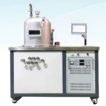
- HFCVD Machine System Equipment for Drawing Die Nano-Diamond Coating
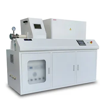
- Chemical Vapor Deposition CVD Equipment System Chamber Slide PECVD Tube Furnace with Liquid Gasifier PECVD Machine
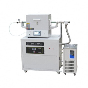
- Split Chamber CVD Tube Furnace with Vacuum Station Chemical Vapor Deposition System Equipment Machine
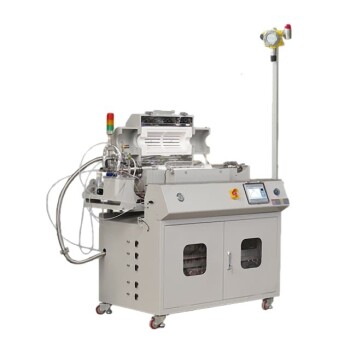
- Multi Heating Zones CVD Tube Furnace Machine Chemical Vapor Deposition Chamber System Equipment
- Customer Made Versatile CVD Tube Furnace Chemical Vapor Deposition Chamber System Equipment
People Also Ask
- Why is Chemical Vapor Deposition (CVD) equipment uniquely suited for constructing hierarchical superhydrophobic structures?
- What types of substrates are used in CVD to facilitate graphene films? Optimize Graphene Growth with the Right Catalyst
- What is the full form of HFCVD? A Guide to Hot Filament Chemical Vapor Deposition
- What is the specific function of the metal filament in HF-CVD? Key Roles in Diamond Growth
- What are the advantages of chemical vapor deposition? Achieve Superior Thin Films for Your Lab
