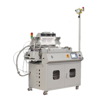
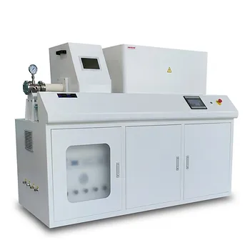
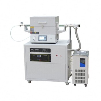
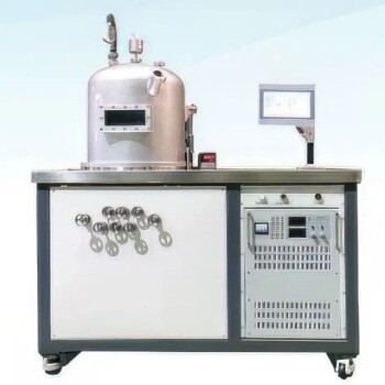
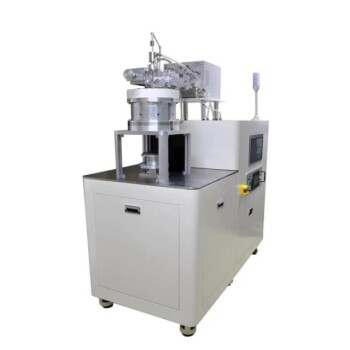
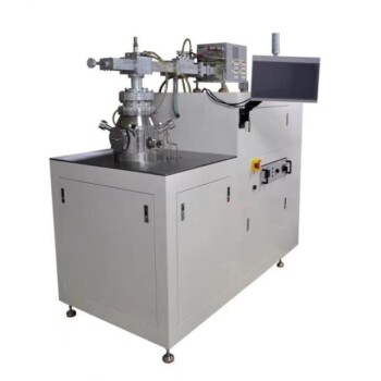
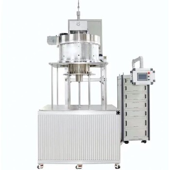
An HDP-CVD reaction chamber functions by utilizing a dual-source radio frequency (RF) system to decouple plasma generation from ion energy. Unlike standard chemical vapor deposition methods, this chamber employs both an inductively coupled RF source and a capacitively coupled RF source simultaneously to independently manipulate the reaction environment.
Core Takeaway: The defining advantage of HDP-CVD is the ability to separate chemical deposition from physical bombardment. By independently controlling the density of the plasma and the energy of the ions striking the wafer, this architecture enables the void-free filling of narrow gaps that standard CVD cannot achieve.
The Dual-RF Source Architecture
The primary differentiator of an HDP-CVD chamber is its use of two distinct RF power sources. This allows operators to fine-tune the deposition process with a level of precision not possible in single-source systems.
Inductive RF Coupling
One RF source is coupled to the plasma inductively. The specific function of this source is to control the plasma density. By increasing the power to this source, the chamber generates a higher concentration of ions and reactive species without necessarily increasing the speed at which they hit the substrate.
Capacitive RF Coupling
The second RF source is coupled to the plasma capacitively. This source is responsible for controlling the ion bombardment energy. It creates a bias that accelerates ions toward the wafer surface, adding a physical component (sputtering or etching) to the chemical deposition process.
Simultaneous Deposition and Etching
By balancing these two sources, the chamber facilitates a process where material is deposited and simultaneously polished (sputtered) by ion bombardment. This prevents the "pinching off" of material at the top of deep trenches, ensuring complete gap filling.
The Underlying CVD Mechanism
While the dual-RF system provides control, the fundamental operation follows established Chemical Vapor Deposition principles.
Precursor Introduction
Mass flow controllers introduce precise amounts of reactant gases (such as silane or organometallics) into the chamber. These gases serve as the volatile precursors that contain the atoms or molecules required for the desired coating.
Chemical Reaction and Adsorption
Once inside the high-density plasma environment, the gases undergo chemical decomposition and reaction. These reactive species transport to the substrate surface, where they adsorb and form a solid, nonvolatile film (commonly dielectrics like silicon dioxide or silicon nitride).
By-product Removal
The chemical reactions that create the solid film also generate volatile by-products. To maintain a clean reaction environment and prevent contamination, these gaseous by-products are continuously desorbed from the surface and removed from the chamber via the exhaust flow.
Understanding the Trade-offs
While HDP-CVD offers superior gap-fill capabilities, the complexity of the chamber introduces specific operational challenges.
Complexity of Process Windows
Because there are two independent RF variables (density vs. bombardment), the "process window"—the range of settings that produce a good result—can be complex to define. You must carefully balance the deposition rate (chemical) against the sputtering rate (physical) to avoid damaging the underlying device structure.
Thermal Management
The generation of high-density plasma naturally results in significant heat generation. The substrate and chamber walls must be managed thermally to prevent defects in the film or stress on the wafer, often requiring sophisticated cooling or temperature control mechanisms within the chamber hardware.
Making the Right Choice for Your Goal
When evaluating HDP-CVD for your fabrication process, align the dual-source capabilities with your specific requirements.
- If your primary focus is Gap Filling: Prioritize the capacitive RF source settings to ensure sufficient ion bombardment is present to keep the trench structure open during fill.
- If your primary focus is Film Quality: Focus on the inductive RF source to maximize plasma density, ensuring a dense, high-quality dielectric film with minimal impurities.
By mastering the interplay between the inductive generation of density and the capacitive control of energy, you transform the reaction chamber from a simple deposition tool into a precision instrument for complex topography management.
Summary Table:
| Feature | Inductive RF Coupling | Capacitive RF Coupling |
|---|---|---|
| Primary Function | Controls Plasma Density | Controls Ion Bombardment Energy |
| Mechanism | Inductive Coupling | Capacitive Bias |
| Process Role | Chemical Deposition Rate | Physical Sputtering/Etching |
| Benefit | High-quality, dense films | Prevents "pinch-off" in narrow gaps |
Elevate Your Thin Film Precision with KINTEK
Unlock the full potential of your fabrication process with KINTEK’s advanced laboratory solutions. Whether you are scaling up semiconductor research or optimizing dielectric deposition, our comprehensive range of high-performance equipment—including CVD and PECVD systems, high-temperature furnaces, and precision cooling solutions—is designed to meet the most rigorous industrial standards.
Why choose KINTEK?
- Expertise in Complex Topography: Specialized tools for void-free gap filling and dense film quality.
- Full Lab Integration: From crushing and milling systems to high-pressure reactors and essential consumables like PTFE and ceramics.
- Targeted Support: We help research labs and manufacturers achieve precise thermal and chemical control.
Contact KINTEK today to optimize your HDP-CVD workflows!
Related Products
- Customer Made Versatile CVD Tube Furnace Chemical Vapor Deposition Chamber System Equipment
- Multi Heating Zones CVD Tube Furnace Machine Chemical Vapor Deposition Chamber System Equipment
- Chemical Vapor Deposition CVD Equipment System Chamber Slide PECVD Tube Furnace with Liquid Gasifier PECVD Machine
- Split Chamber CVD Tube Furnace with Vacuum Station Chemical Vapor Deposition System Equipment Machine
- HFCVD Machine System Equipment for Drawing Die Nano-Diamond Coating
People Also Ask
- What is the function of a high-temperature CVD tube furnace in 3D graphene foam prep? Master 3D Nanomaterial Growth
- What is chemical vapor deposition for CNT? The Leading Method for Scalable Carbon Nanotube Synthesis
- What is the difference between hot wall CVD and cold wall CVD? Choose the Right System for Your Process
- What is the synthesis and mechanism involved in the preparation of carbon nanotubes using CVD process? Master Controlled Growth for Your Application
- How does a CVD tube furnace inhibit the sintering of silver supports? Boost Membrane Durability and Performance
