RF sputtering is a highly versatile deposition technique capable of processing virtually any material type. While it is technically suitable for both conductive and non-conductive substances, it is most distinctively and commonly employed for depositing dielectric (insulating) sputtering target materials.
The Core Takeaway While RF sputtering works on all materials, it is the industry standard for non-conductive dielectrics which cannot be processed using standard DC methods. If your target material is an electrical insulator, RF sputtering is the requisite choice.
The Primary Application: Dielectrics
RF sputtering fills a specific gap in thin-film deposition that other methods cannot address.
Focusing on Non-Conductive Targets
The most critical application of RF sputtering is the deposition of dielectric materials.
These are materials that do not conduct electricity. Standard DC sputtering requires a conductive path through the target material to sustain the plasma discharge.
Because dielectrics act as insulators, they require the alternating current (AC) approach of RF sputtering to prevent charge build-up and allow the sputtering process to occur.
Universal Compatibility
According to the primary technical guidelines, RF sputtering is suitable for all material types.
This includes both conductive metals and complex non-conductive compounds.
However, just because it can process conductive materials does not always mean it is the primary choice for them (see the "Trade-offs" section below).
Substrate and Surface Versatility
Beyond the target material being sputtered, RF sputtering is also defined by the types of materials it can deposit onto.
Heat-Sensitive Materials
The technique generates a minimal thermal load compared to other deposition methods.
This allows for deposition onto heat-sensitive substrates that might otherwise warp or degrade, such as plastics or certain polymers.
Unusual Surfaces
The process is compatible with a wide variety of surface types.
This includes standard rigid substrates like glass and metals. It also extends to flexible or unconventional materials, including textiles.
Understanding the Trade-offs
While RF sputtering is the "universal" solution, it is not always the most efficient choice for every project.
When to Use DC Sputtering Instead
If your target material is electrically conductive, RF sputtering is technically possible but often unnecessary.
For pure metals such as Iron (Fe), Copper (Cu), and Nickel (Ni), DC sputtering is generally preferred.
DC power is cited as a more effective and economical method for conductive targets. RF sputtering involves more complex power sources (typically fixed at 13.56 MHz) and lower deposition rates, making it less efficient for simple metal deposition.
Making the Right Choice for Your Goal
Select your deposition method based on the electrical properties of your target material:
- If your target is a non-conductive insulator: You must use RF Sputtering, as it is the standard solution for dielectric materials.
- If your target is a conductive metal (Fe, Cu, Ni): You should generally use DC Sputtering, as it is more economical and effective for conductors.
- If your substrate is highly heat-sensitive: You should lean toward RF/Magnetron Sputtering due to its lower thermal load.
RF sputtering removes the electrical limitations of your materials, allowing you to deposit high-quality thin films regardless of conductivity.
Summary Table:
| Material Category | Suitability | Preferred Method | Key Application Examples |
|---|---|---|---|
| Dielectrics (Insulators) | Excellent | RF Sputtering | Ceramics, Oxides, Nitrides |
| Conductive Metals | Possible | DC Sputtering | Iron (Fe), Copper (Cu), Nickel (Ni) |
| Heat-Sensitive Substrates | Excellent | RF Sputtering | Plastics, Polymers, Textiles |
| Rigid Substrates | Excellent | Either | Glass, Silicon Wafers, Metals |
Elevate Your Material Research with KINTEK’s Precision Solutions
Unlock the full potential of your thin-film applications with KINTEK’s advanced laboratory equipment. Whether you are depositing complex non-conductive dielectrics using RF sputtering or working with conductive metals, we provide the high-performance tools you need for superior results.
Beyond sputtering solutions, KINTEK specializes in a comprehensive range of laboratory equipment, including high-temperature furnaces (muffle, vacuum, CVD), hydraulic presses, and high-pressure reactors. We support global research facilities with high-quality consumables like PTFE products, ceramics, and crucibles designed to withstand the most demanding environments.
Ready to optimize your lab's efficiency? Contact us today to discuss your specific requirements and see how our expertise can drive your innovation forward!
Related Products
- RF PECVD System Radio Frequency Plasma-Enhanced Chemical Vapor Deposition RF PECVD
- Horizontal High Temperature Graphite Vacuum Graphitization Furnace
- Spark Plasma Sintering Furnace SPS Furnace
- Automatic Laboratory Hydraulic Press for XRF & KBR Pellet Press
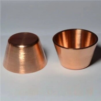
- Electron Beam Evaporation Coating Oxygen-Free Copper Crucible and Evaporation Boat
People Also Ask
- What is plasma enhanced chemical vapour deposition PECVD used for? Enable Low-Temp Thin Films for Electronics & Solar
- What is the role of RF-PECVD in VFG preparation? Mastering Vertical Growth and Surface Functionality
- What is plasma CVD? Unlock Low-Temperature Thin Film Deposition for Sensitive Materials
- How does plasma enhance CVD? Unlock Low-Temperature, High-Quality Film Deposition
- What is plasma enhanced chemical vapour deposition process? Unlock Low-Temperature, High-Quality Thin Films


