Electrolytic polishing serves to drastically transform the surface quality of copper foils prior to the chemical vapor deposition (CVD) process. Its primary function is to minimize surface roughness while simultaneously stripping away native oxide layers and other impurities. By creating an atomically flat and clean substrate, this step ensures the copper is physically and chemically prepared to host sensitive nanomaterials.
By eliminating microscopic irregularities and surface contaminants, electrolytic polishing creates the ideal environment for material growth. This pristine surface is a strict requirement for producing large-area, continuous, and low-defect layers of graphene and hexagonal boron nitride (hBN).
The Critical Role of Substrate Preparation
Reducing Surface Roughness
Commercial copper foil, while cost-effective for mass production, inherently possesses a rough surface texture. Electrolytic polishing levels these microscopic peaks and valleys to create an extremely flat topography.
Because graphene and hBN are single-atom thick materials, they conform tightly to the substrate; any underlying roughness can induce strain or structural defects in the growing lattice.
Eliminating Impurities and Oxides
Copper is highly reactive and naturally forms an oxide layer when exposed to air. This layer, along with other surface contaminants, acts as a barrier that interferes with the nucleation process during CVD.
Electrolytic polishing chemically removes this oxide layer and strips away surface impurities. This exposes pristine copper atoms, facilitating a direct and uniform interaction with the precursor gases used to grow 2D materials.
Enabling Continuous, Large-Area Growth
Achieving a continuous, single-layer film over a large area is notoriously difficult on untreated surfaces. Defects in the substrate often lead to grain boundaries or holes in the final material.
The high-quality surface produced by polishing promotes uniform nucleation. This uniformity is essential for growing cohesive sheets of material rather than fragmented patches, a key factor in utilizing CVD for scalable production.
Ensuring Accurate Performance Comparisons
When researching the barrier performance of materials like graphene versus hBN, variables must be strictly controlled. If the substrate is rough or dirty, defects in the 2D material will compromise its barrier properties.
Polishing ensures that any difference in performance is due to the intrinsic properties of the graphene or hBN, rather than artifacts caused by a poor-quality copper substrate.
Understanding the Challenges
Process Sensitivity
While electrolytic polishing improves quality, it introduces a sensitive time constraint to the manufacturing workflow. Once the oxide layer is stripped, the highly reactive copper surface is vulnerable to rapid re-oxidation.
Handling Requirements
To maintain the benefits of the polish, the substrate must be handled with extreme care and typically introduced into the CVD vacuum chamber immediately after processing. Any delay or mishandling can negate the benefits of the polishing step, reintroducing contaminants that the process just removed.
Making the Right Choice for Your Goal
Whether you are conducting high-precision research or developing manufacturing protocols, the quality of your substrate dictates your results.
- If your primary focus is high-fidelity material characterization: You must utilize electrolytic polishing to ensure that defect densities are minimized and barrier performance data is accurate.
- If your primary focus is mass production viability: You should recognize that while copper is a cost-effective substrate, achieving high-quality yields likely requires integrating a polishing step into the workflow.
The integrity of a two-dimensional material is defined by the quality of the surface it grows on.
Summary Table:
| Feature | Impact of Electrolytic Polishing | Benefit for CVD Growth |
|---|---|---|
| Surface Roughness | Reduces microscopic peaks and valleys | Minimizes lattice strain and structural defects |
| Oxide Layers | Chemically strips native copper oxides | Promotes uniform nucleation and precursor interaction |
| Surface Purity | Removes organic and metallic contaminants | Prevents formation of holes and unwanted grain boundaries |
| Film Continuity | Creates an atomically flat topography | Facilitates large-area, cohesive 2D material sheets |
| Material Integrity | Ensures a pristine substrate interface | Allows for accurate intrinsic performance characterization |
Elevate Your Nanomaterial Research with KINTEK Precision
The quality of your 2D materials depends entirely on the substrate. At KINTEK, we specialize in the high-performance laboratory equipment necessary to achieve these exacting standards. From advanced CVD and PECVD systems to specialized electrolytic cells and electrodes, our solutions are designed to help you produce flawless, large-area graphene and hBN.
Whether you are refining high-temperature furnace protocols or scaling up production with our hydraulic presses and crushing systems, KINTEK provides the comprehensive tools and high-purity consumables—like PTFE products and ceramics—that researchers trust.
Ready to eliminate defects and optimize your material growth? Contact KINTEK today to discover how our expertise can enhance your lab's efficiency and results.
References
- Miriam Galbiati, Luca Camilli. Real-time oxide evolution of copper protected by graphene and boron nitride barriers. DOI: 10.1038/srep39770
This article is also based on technical information from Kintek Solution Knowledge Base .
Related Products
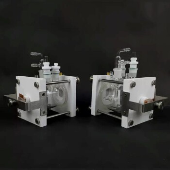
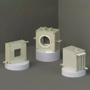
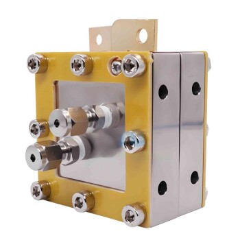
- Electrode Polishing Material for Electrochemical Experiments
- Electrolytic Electrochemical Cell for Coating Evaluation
- Electrolytic Electrochemical Cell with Five-Port
- Flat Corrosion Electrolytic Electrochemical Cell
- Quartz Electrolytic Electrochemical Cell for Electrochemical Experiments
People Also Ask
- What is the correct technique for polishing an electrode? Master the Steps for Reliable Electrochemical Data
- Which types of materials are basically polished by electrolytic polishing? A Guide to Metals & Alloys
- How do you prepare the polishing setup for an electrode? Achieve a Flawless Mirror Finish for Reliable Electrochemistry
- What is the general procedure and what precautions should be taken during the polishing process? Achieve a Flawless Electrode Finish
- What criteria are used during the visual inspection of electrodes? Essential Quality Assessment for Your Lab