High Temperature Chemical Vapour Deposition (HTCVD) is a specialized manufacturing process primarily used for the growth of Silicon Carbide (SiC) crystals.
Operating within a closed reactor, this method utilizes mixed reaction gases that decompose at extreme temperatures to deposit solid crystal films onto a substrate. It is a critical technology for producing the high-quality semiconductor materials required for modern electronics.
Core Takeaway: HTCVD distinguishes itself by operating at extreme thermal ranges (2000°C–2300°C) to bridge the gap between gas-phase precursors and solid-state bulk crystal formation. While it offers rapid deposition rates for difficult materials like Silicon Carbide, precise control is required to prevent structural defects.
The Mechanics of the Process
To understand why HTCVD is chosen over other methods, you must understand the extreme environment it creates. It is not merely "hot"; it operates at temperatures where many other materials would melt or degrade.
Extreme Thermal Environment
The defining feature of HTCVD is the operating temperature. The process is conducted in a closed reactor where external heating maintains the chamber between 2000°C and 2300°C.
Gas-Phase Decomposition
The process begins when a mixed reaction gas is introduced into this heated chamber. Upon reaching the substrate, the high temperature forces the gas to decompose.
Surface Chemical Reaction
Once decomposed, the chemical components react on the surface of the substrate. This reaction generates a solid crystal film, effectively growing the material layer by layer.
Continuous Regeneration
As the solid product forms and detaches from the gas phase, new reaction gas is continuously introduced. This allows the crystal film to continue growing uninterrupted, facilitating the creation of substantial crystal structures.
Understanding the Trade-offs
While HTCVD is a powerful tool for growing Silicon Carbide, it is not without significant engineering challenges. The relationship between speed and quality is the primary tension in this process.
Deposition Rate vs. Crystal Quality
One of the main benefits of HTCVD is the potential for fast deposition rates. However, speed comes at a cost.
Structural Defects
If the deposition occurs too quickly or without precise control, the resulting crystal structure can suffer. Common issues include loose crystals and the formation of coarse grains.
Dendritic Crystallization
In scenarios where process parameters are not strictly regulated, the material may exhibit dendritic crystallization. This results in tree-like branching structures rather than the solid, uniform single crystal required for high-performance semiconductor applications.
Making the Right Choice for Your Goal
HTCVD is a targeted solution for specific material challenges. It is not a general-purpose coating method but a specialized growth technique.
- If your primary focus is Silicon Carbide (SiC) production: HTCVD is the standard for growing these crystals due to its ability to handle the extreme temperatures required for SiC formation.
- If your primary focus is avoiding structural defects: You must prioritize thermal regulation and gas flow control over deposition speed to prevent coarse grains and dendritic growth.
Success with HTCVD requires balancing the efficiency of high deposition rates with the stringent stability needed for high-purity crystal structures.
Summary Table:
| Feature | HTCVD Specification |
|---|---|
| Primary Application | Silicon Carbide (SiC) Crystal Growth |
| Operating Temperature | 2000°C to 2300°C |
| Process Mechanism | Gas-phase decomposition & surface reaction |
| Output Material | Solid crystal films & bulk crystals |
| Key Advantage | Rapid deposition rates for difficult materials |
| Critical Challenge | Preventing structural defects and dendritic growth |
Elevate Your Semiconductor Research with KINTEK
Precision in High Temperature Chemical Vapour Deposition (HTCVD) requires equipment that can withstand extreme thermal environments without compromising crystal purity. KINTEK specializes in advanced laboratory solutions, providing the high-performance CVD, PECVD, and atmosphere furnaces necessary for successful Silicon Carbide (SiC) production.
Whether you are scaling up semiconductor manufacturing or conducting specialized material research, our comprehensive range of high-temperature systems and essential consumables—including ceramics, crucibles, and cooling solutions—ensures stable, repeatable results.
Ready to optimize your deposition rates and eliminate structural defects? Contact KINTEK today to discuss your project requirements with our technical experts.
Related Products
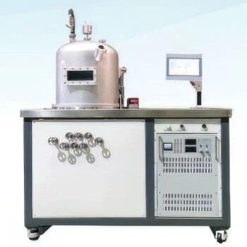
- HFCVD Machine System Equipment for Drawing Die Nano-Diamond Coating
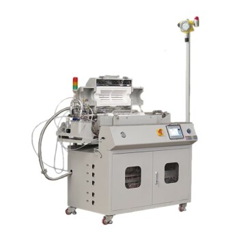
- Multi Heating Zones CVD Tube Furnace Machine Chemical Vapor Deposition Chamber System Equipment
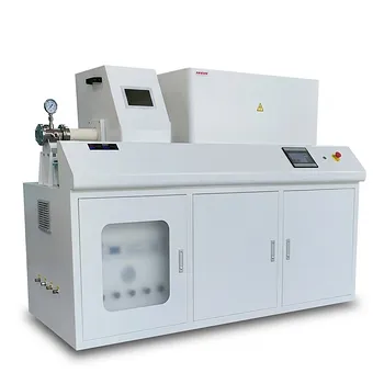
- Customer Made Versatile CVD Tube Furnace Chemical Vapor Deposition Chamber System Equipment
- Chemical Vapor Deposition CVD Equipment System Chamber Slide PECVD Tube Furnace with Liquid Gasifier PECVD Machine
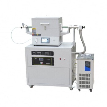
- Split Chamber CVD Tube Furnace with Vacuum Station Chemical Vapor Deposition System Equipment Machine
People Also Ask
- What are the advantages of chemical vapor deposition? Achieve Superior Thin Films for Your Lab
- Why is Chemical Vapor Deposition (CVD) equipment uniquely suited for constructing hierarchical superhydrophobic structures?
- What is the full form of HFCVD? A Guide to Hot Filament Chemical Vapor Deposition
- What is the function of tungsten filaments in HFCVD? Powering Diamond Film Synthesis with Thermal Excitation
- How expensive is chemical vapor deposition? Understanding the True Cost of High-Performance Coating
