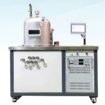
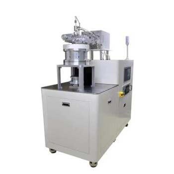
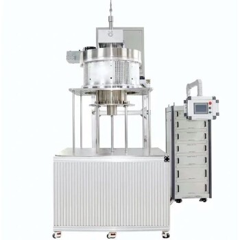
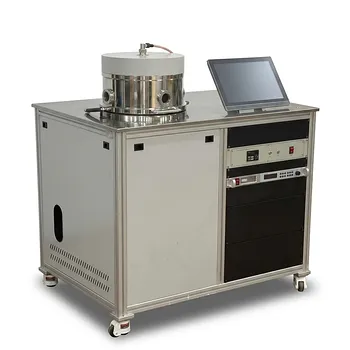
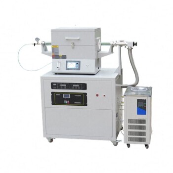
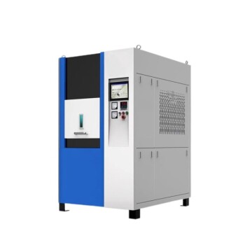
High-Density Plasma CVD (HDP-CVD) is specifically applied in semiconductor manufacturing to create high-quality dielectric films essential for devices with challenging geometries. Its primary utility lies in depositing insulation layers for Shallow Trench Isolation (STI), Interlayer Dielectrics (ILD), and Pre-metal Dielectrics (PMD).
HDP-CVD serves as a critical gapless fill solution for logic applications and advanced memory processing. It is the definitive choice for insulating high-aspect-ratio structures where maintaining a void-free material is essential for device performance.
The Core Function: Gap Filling in Advanced Architectures
Tackling High Aspect Ratios
Modern semiconductor devices are built with deep, narrow features known as high aspect ratios. HDP-CVD is specifically engineered to address the geometry of these structures. It allows manufacturers to deposit material into these deep trenches without blockage.
Ensuring Void-Free Deposition
The primary technical requirement in these advanced nodes is a "gapless fill." If a dielectric film fails to completely fill a trench, it leaves air gaps or "voids" that compromise the chip. HDP-CVD provides a high-density solution that eliminates these defects in both logic and memory devices.
Specific Manufacturing Applications
Shallow Trench Isolation (STI)
STI is a fundamental application used to electrically separate active components on a silicon wafer. HDP-CVD is utilized here to fill the isolation trenches with a robust dielectric material. This ensures that current does not leak between adjacent transistors.
Interlayer Dielectrics (ILD)
As chips are constructed in vertical layers, conductive metal lines must be insulated from one another. HDP-CVD deposits the Interlayer Dielectrics (ILD) required to separate these levels. This application is critical for preventing short circuits in multi-level interconnect structures.
Pre-metal Dielectrics (PMD)
The PMD layer acts as a barrier between the silicon transistors and the very first layer of metal wiring. HDP-CVD is employed to deposit this insulation layer before metallization begins. It ensures the delicate transistor gates are fully protected and electrically isolated.
The Trade-off: Why Standard Deposition Falls Short
The Limitation of Conventional CVD
Standard Chemical Vapor Deposition (CVD) methods often struggle as device dimensions shrink. When faced with high aspect ratios, conventional methods may pinch off the top of a trench before the bottom is filled.
The Necessity of High-Density Plasma
HDP-CVD is required specifically when the geometry becomes too aggressive for standard tools. While it is a more advanced process, it is necessary to avoid the structural weaknesses and reliability issues caused by incomplete gap filling in advanced memory and logic chips.
Making the Right Choice for Your Process
If you are determining where to insert HDP-CVD into your process flow, consider the specific structural requirements of your device:
- If your primary focus is component isolation: Implement HDP-CVD for Shallow Trench Isolation (STI) to guarantee gapless barriers between active areas on the wafer.
- If your primary focus is vertical interconnects: Utilize this technology for Pre-metal (PMD) and Interlayer Dielectrics (ILD) to ensure solid, high-quality insulation between conductive layers in high-aspect-ratio designs.
HDP-CVD remains the standard for achieving structural integrity in the most geometrically challenging layers of modern semiconductor fabrication.
Summary Table:
| Application Type | Primary Purpose | Key Benefit in Semiconductor Fabrication |
|---|---|---|
| Shallow Trench Isolation (STI) | Component Isolation | Electrically separates active components with robust dielectric fill. |
| Interlayer Dielectrics (ILD) | Vertical Insulation | Separates multi-level metal interconnects to prevent short circuits. |
| Pre-metal Dielectrics (PMD) | Transistor Protection | Provides a barrier between silicon transistors and the first metal layer. |
| Gap-Fill Solutions | Structural Integrity | Ensures void-free material deposition in deep, narrow high-aspect-ratio features. |
Elevate Your Semiconductor Fabrication with KINTEK Precision
Are you struggling with voids or incomplete gap filling in high-aspect-ratio structures? KINTEK specializes in advanced laboratory and thin-film solutions, providing the high-quality equipment and consumables needed for cutting-edge material research.
Our extensive portfolio includes PECVD, CVD, and MPCVD systems, as well as high-temperature furnaces and essential consumables like ceramics and crucibles. Whether you are optimizing STI, ILD, or PMD processes, our technical experts are ready to provide the tools and support you need for defect-free results.
Ready to achieve superior structural integrity? Contact us today to discuss your project requirements!
Related Products
- HFCVD Machine System Equipment for Drawing Die Nano-Diamond Coating
- Microwave Plasma Chemical Vapor Deposition MPCVD Machine System Reactor for Lab and Diamond Growth
- 915MHz MPCVD Diamond Machine Microwave Plasma Chemical Vapor Deposition System Reactor
- Inclined Rotary Plasma Enhanced Chemical Vapor Deposition PECVD Equipment Tube Furnace Machine
- Chemical Vapor Deposition CVD Equipment System Chamber Slide PECVD Tube Furnace with Liquid Gasifier PECVD Machine
People Also Ask
- What types of substrates are used in CVD to facilitate graphene films? Optimize Graphene Growth with the Right Catalyst
- What are the disadvantages and challenges of the HFCVD method? Overcome Growth Limits and Filament Issues
- What are the advantages of chemical vapor deposition? Achieve Superior Thin Films for Your Lab
- How expensive is chemical vapor deposition? Understanding the True Cost of High-Performance Coating
- What is the full form of HFCVD? A Guide to Hot Filament Chemical Vapor Deposition
