Process-induced damage during deposition manifests primarily through three mechanisms: ion bombardment, chemical contamination, and ultraviolet (UV) radiation. Assessing this damage is notoriously difficult because the effects are often too subtle to observe immediately, usually requiring the lengthy completion of device fabrication and testing before the problem becomes visible.
Core Takeaway As device features shrink, they become increasingly sensitive to complex, multi-source damage mechanisms. The primary challenge lies in the "lag" between deposition and detection, as subtle defects often remain invisible until the final stages of device testing.
The Mechanics of Deposition Damage
Ion Bombardment
During deposition, the substrate is often exposed to energetic particles. The physical impact of these ions can disrupt the material structure or create physical defects on the surface.
Chemical Contamination
The introduction of foreign materials during the process is a constant risk. Even microscopic levels of contamination can alter the electrical properties of the device layer.
Ultraviolet (UV) Radiation
High-energy light generated during the process poses a significant threat. This radiation can penetrate sensitive layers, potentially damaging the material's internal bonding or charge states.
Simultaneous Exposure
These damage sources rarely occur in isolation. Multiple mechanisms—physical, chemical, and radiative—can be active at the exact same time, compounding the severity of the damage.
Why Assessment is a Challenge
The Subtlety of Defects
The damage inflicted is not always physically obvious. It is often a "soft" failure that does not present a visible structural break, making it invisible to standard optical inspection.
Complex Causality
Because mechanisms overlap, identifying the root cause is difficult. It is challenging to determine if a failure resulted specifically from ion impact or UV exposure when both were present.
The Fabrication Lag
This is the most critical hurdle for engineers. You often cannot detect the damage immediately after the deposition step.
Requirement for Full Testing
To observe the actual impact of the damage, you typically must finish fabricating the device. Only after the completed unit undergoes electrical testing do the performance issues reveal themselves.
Understanding the Trade-offs
Feature Size vs. Sensitivity
There is an inverse relationship between feature size and durability. As device features shrink to improve performance, their sensitivity to process-induced damage increases disproportionately.
Detection Speed vs. Accuracy
Rapid inspection tools may miss these subtle defects entirely. The only way to get an accurate assessment is through the time-consuming process of full-flow fabrication, which slows down process development cycles.
Managing Process Risk in Fabrication
While you cannot eliminate all risks, understanding the nature of these mechanisms allows for better diagnosis.
- If your primary focus is Root Cause Analysis: Remember that multiple sources (UV, ions, contamination) likely acted simultaneously, rather than a single isolated event.
- If your primary focus is Process Development: Anticipate a long feedback loop, as reliable data will likely only come from testing fully fabricated devices.
Recognizing the invisibility of these defects is the first step toward effective mitigation.
Summary Table:
| Damage Type | Mechanism | Impact on Device |
|---|---|---|
| Ion Bombardment | Physical impact of energetic particles | Structural disruption and surface defects |
| Chemical Contamination | Introduction of foreign materials | Alteration of electrical properties |
| UV Radiation | High-energy light penetration | Damage to internal bonding or charge states |
| Synergistic Effects | Simultaneous multi-source exposure | Compounded material degradation |
Precision Equipment for Damage-Free Fabrication
Process-induced damage can halt your progress, especially as device features shrink. At KINTEK, we understand the delicate balance between deposition efficiency and material integrity. Our comprehensive range of CVD, PECVD, and MPCVD systems, alongside our high-temperature furnaces and vacuum solutions, are engineered to provide the precise control needed to mitigate ion bombardment and UV risks.
Whether you are conducting battery research, developing advanced semiconductors, or refining dental ceramics, KINTEK provides the laboratory equipment and high-purity consumables—like crucibles, ceramics, and PTFE products—that ensure your results are consistent and reproducible. Don't wait for final testing to find defects; invest in equipment built for excellence.
Ready to elevate your laboratory's capabilities? Contact KINTEK experts today for a tailored solution.
Related Products
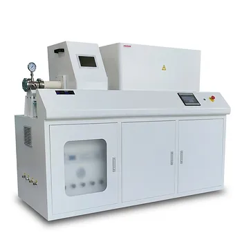
- Chemical Vapor Deposition CVD Equipment System Chamber Slide PECVD Tube Furnace with Liquid Gasifier PECVD Machine
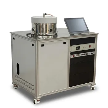
- RF PECVD System Radio Frequency Plasma-Enhanced Chemical Vapor Deposition RF PECVD
- Customer Made Versatile CVD Tube Furnace Chemical Vapor Deposition Chamber System Equipment
- Inclined Rotary Plasma Enhanced Chemical Vapor Deposition PECVD Equipment Tube Furnace Machine
- Inclined Rotary Plasma Enhanced Chemical Vapor Deposition PECVD Equipment Tube Furnace Machine
People Also Ask
- What are the core advantages of PE-CVD in OLED encapsulation? Protect Sensitive Layers with Low-Temp Film Deposition
- How are carbon nanotubes grown? Master Scalable Production with Chemical Vapor Deposition
- How expensive is chemical vapor deposition? Understanding the True Cost of High-Performance Coating
- What is plasma enhanced chemical vapor deposition PECVD equipment? A Guide to Low-Temperature Thin Film Deposition
- What is the chemical vapor deposition growth process? Build Superior Thin Films from the Atom Up
