All Questions
What Techniques Can Be Used To Improve The Quality Of Cvd Graphene Growth? Expert Methods For High-Quality Graphene
Master CVD graphene quality through substrate pre-treatment, cold wall CVD systems, and precise control of gas purity and temperature regulation.
Why Is It Difficult To Achieve A Completely Uniform Layer Of Graphene On A Substrate Using Cvd? Mastering Graphene Growth
Understand the fluid dynamics and reactant depletion challenges in CVD graphene growth and how to overcome them for superior uniformity.
What Methods Separate Cvd Graphene From Its Substrate? Optimize Your Transfer Process With Advanced Techniques
Explore CVD graphene separation methods: chemical etching, PMMA-assisted transfer, and intercalation to ensure high-quality material integrity.
What Is A Primary Challenge In Producing Usable Graphene Sheets After Cvd? Overcoming The Transfer Bottleneck
Learn why separating graphene from its growth substrate is the biggest challenge in CVD production and how to preserve its structural integrity.
What Is A Potential Complication Of Using Catalysts In The Cvd Process For Graphene? Mastering Carbon Solubility
Understand how carbon solubility in CVD metal catalysts impacts graphene quality and how to control unwanted precipitation.
Why Are Metal Catalysts Essential For Creating Graphene Via The Cvd Process? Unlock High-Quality Graphene Synthesis
Learn how metal catalysts lower reaction temperatures and act as structural templates for high-quality graphene production via CVD processes.
What Are The Two Fundamental Steps In The Creation Of Cvd Graphene? Master Pyrolysis And Structure Formation
Learn how precursor pyrolysis and carbon structure formation drive CVD graphene synthesis, and the critical role of catalysts in high-quality labs.
What Is A Major Disadvantage Of The Chemical Vapor Deposition (Cvd) Process? Overcoming Safety And Thermal Challenges
Learn about the primary drawbacks of CVD, including toxic by-product generation and high-temperature limitations for substrates.
What Is Ultra-High Vacuum Cvd (Uhvcvd)? Achieve Superior Purity In Advanced Material Deposition
Learn about UHVCVD, its 10⁻⁶ Pa vacuum environment, and why it is the gold standard for high-purity material growth in semiconductor research.
What Is Low Pressure Cvd (Lpcvd) And What Are Its Advantages? Enhance Film Uniformity & Protect Sensitive Substrates
Learn how Low Pressure CVD (LPCVD) improves film uniformity and prevents thermal damage. Discover its advantages over APCVD and PECVD methods.
What Are The Two Main Categories Of Modern Cvd Processes? Comparing Lpcvd And Uhvcvd For Precision Film Growth
Learn the differences between LPCVD and UHVCVD, focusing on operating pressures, film uniformity, and high-purity applications in modern industry.
What Are The Benefits And Characteristics Of Coatings Produced By Chemical Vapor Deposition (Cvd)? | High-Purity Solutions
Unlock the benefits of CVD: high-purity, uniform, and ultra-hard coatings for complex geometries. Perfect for semiconductors and high-wear parts.
What Is The Primary Condition That Defines The Type Of Reaction In Cvd? Master Substrate Temperature Control
Learn why substrate temperature is the critical variable in CVD, influencing reaction pathways, film quality, and thermodynamic stability.
How Does The General Process Of Chemical Vapor Deposition (Cvd) Work? Mastering Thin-Film Uniformity
Learn how Chemical Vapor Deposition (CVD) transforms gaseous precursors into high-purity solid films through precise thermal chemical reactions.
What Are The Critical Parameters For High-Quality Cvd Graphene? Optimize Your Synthesis Process
Master CVD graphene quality by controlling temperature, gas flow, and substrate preparation for defect-free, single-layer results.
What Is Chemical Vapor Deposition (Cvd) In Graphene? Scale High-Quality Monolayer Production
Learn how CVD enables large-scale, high-purity graphene synthesis. Explore the bottom-up process, substrate roles, and industrial advantages.
What Is The Process Of Chemical Vapor Deposition (Cvd)? Master High-Purity Thin Film Coatings
Learn the step-by-step CVD process, from precursor transport to surface reaction, and discover how to achieve superior film uniformity and purity.
What Are The Two Main Types Of Vapor Deposition Systems? Pvd Vs. Cvd Explained
Learn the differences between PVD and CVD vapor deposition systems, including their mechanics, thermal requirements, and substrate compatibility.
What Industries Utilize The Vacuum Deposition Process? Unlocking Precision In Electronics, Energy, And Healthcare
Explore how vacuum deposition drives innovation in solar cells, LED displays, and medical devices through high-purity thin-film coating technology.
How Does The Quality Of Modern Hpht And Cvd Diamonds Compare? Achieve Flawless Results With Precision Lab Technology
Discover the truth about HPHT vs. CVD diamonds. Learn why modern technology makes them visually identical and how to choose based on growth traits.
How Do The Growth Patterns Of Hpht, Cvd, And Natural Diamonds Differ? Uncover The Morphology Of Lab Vs. Mined Gems
Discover the structural differences between HPHT, CVD, and natural diamonds, including unique morphologies and growth directions for identification.
What Are The Typical Characteristics And Inclusions Found In Cvd Diamonds? Identify The Unique Fingerprints
Learn the key traits of CVD diamonds, from graphite inclusions and silicon traces to the absence of metal flux and internal graining patterns.
What Are The Advantages Of The Cvd Diamond Growing Process Compared To The Hpht Process? Master Precision & Efficiency
Discover why CVD diamond growth excels with lower costs, superior chemical control, and scalability compared to high-pressure HPHT methods.
What Is The Chemical Vapour Deposition (Cvd) Method For Growing Diamonds? Discover Precision Carbon Synthesis
Learn how the CVD diamond growth process works, from plasma ionization to atom-by-atom deposition, and why it's the top choice for pure crystals.
What Are The Modern Applications Of Cvd-Grown Graphene? Exploring Advanced Electronics And Energy Solutions
Learn how CVD-grown graphene is revolutionizing electronics, optoelectronics, and thermal management with high-purity, large-area 2D films.
What Are Some Examples Of Solid And Gaseous Precursors Used In The Cvd Of Graphene? Optimize Your Synthesis Process
Learn about gaseous and solid precursors for graphene CVD, from standard methane to sustainable waste plastics and low-temp hexachlorobenzene.
What Types Of Carbon Sources Are Used For The Cvd Of Graphene? Optimize Your Synthesis With The Right Precursors
Learn how solid, liquid, and gaseous carbon sources like methane influence graphene quality in Thermal and Plasma-Enhanced CVD processes.
What Are Some Examples Of Growing Graphene On Polycrystalline Metals Using Cvd? Master Large-Scale Graphene Synthesis
Learn how polycrystalline metals like Cu, Ni, Fe, and Co dictate graphene thickness and uniformity in Chemical Vapor Deposition (CVD) processes.
Can Monocrystalline Graphene Be Grown On Polycrystalline Metal Substrates? Unlock High-Quality Cvd Graphene Synthesis
Learn how CVD enables monocrystalline graphene growth on polycrystalline metals like Cu and Ni through precise annealing and cooling protocols.
What Is A Key Advantage Of Using Silicon Carbide (Sic) As A Substrate For Cvd Graphene Growth? Achieve Free-Standing Graphene
Learn why Silicon Carbide (SiC) substrates enable low-temperature CVD graphene growth, preventing pinning points for superior material quality.
Why Are Transition Metals Other Than Co, Ni, And Cu Less Favorable For Cvd Graphene? Costs & Technical Hurdles
Explore why precious metals like Pt and Au fall short in CVD graphene production due to high costs, scalability issues, and transfer challenges.
Which Substrates Are Considered Superior For The Cvd Of Graphene? Choosing Copper Vs. Nickel For High-Quality Growth
Discover why copper and nickel are the top substrates for graphene CVD, offering precise layer control, scalability, and high-quality results.
Why Is Cvd The Most Efficient Method For Preparing Graphene? Unlock Scalable, High-Quality Material Production
Learn why Chemical Vapor Deposition (CVD) is the industrial standard for large-scale, high-quality, and cost-effective graphene synthesis.
What Are The Different Types Of Chemical Vapor Deposition (Cvd) Methods? Choose The Right Process For Your Lab
Explore the various CVD methods categorized by pressure, precursor state, and energy source to optimize your thin-film deposition efficiency.
What Is The General Process Of Chemical Vapor Deposition (Cvd)? Master High-Performance Thin-Film Growth
Learn how Chemical Vapor Deposition (CVD) uses precursor reactions in a vacuum to create high-purity, conformal coatings on complex geometries.
What Types Of Substrates Are Used In Cvd To Facilitate Graphene Films? Optimize Graphene Growth With The Right Catalyst
Learn why copper, nickel, and cobalt are essential substrates for CVD graphene production and how they control film thickness and quality.
For What Purposes Is Chemical Vapor Deposition (Cvd) Considered An Efficient Technique? Unlock High-Performance Coatings
Learn why CVD is the gold standard for high-purity graphene, semiconductors, and uniform coatings on complex industrial geometries.
What Potential New Method For Synthesizing Large-Area Diamond Is Suggested? Explore Low-Pressure Phase Transitions
Discover how a new graphite-to-diamond phase transition mechanism could revolutionize large-area diamond synthesis at low pressures.
How Does The Newly Proposed Diamond Formation Mechanism Challenge The Conventional Understanding? | Cvd Innovation
Discover how graphite's role in CVD has shifted from a contaminant to an essential precursor, revolutionizing the theory of diamond synthesis.
What Is The Newly Discovered Mechanism For Diamond Formation During Cvd? Explore The Graphite-To-Diamond Transition
Discover how a Hydrogen-Oxygen-Tantalum atmosphere enables a phase transition from graphene and graphite needles into high-purity sp3 diamond.
Why Does The Growth Of Additional Graphene Layers Typically Not Occur? Unlock Self-Limiting Synthesis Secrets
Understand why graphene growth halts after a monolayer forms due to catalyst passivation and the inert nature of the graphene lattice.
How Does A Continuous, Single Layer Of Graphene Form From Carbon Species? Master The 4 Stages Of Graphene Growth
Understand the process of graphene formation: from surface diffusion and nucleation to edge-driven growth for a perfect, continuous single layer.
What Occurs During The Chemical Vapor Deposition (Cvd) Process For Graphene Growth? A Guide To High-Quality Synthesis
Learn the CVD process for graphene: from gas decomposition on catalysts to lattice formation, ensuring high-quality, large-area monolayer growth.
What Is The Purpose Of Using Metal Catalyst Substrates In Graphene Manufacturing? Lower Thermal Energy Thresholds
Learn how metal catalyst substrates enable energy-efficient graphene production by lowering pyrolytic decomposition temperatures below 1000 °C.
What Is Pyrolysis In The Context Of Single-Layer Graphene Manufacturing? Overcoming The 1000°C Thermal Barrier
Learn how pyrolysis breaks down carbon precursors at 1000°C+ to enable single-layer graphene growth and the engineering challenges involved.
What Is Chemical Vapor Deposition (Cvd)? Master High-Purity Thin Film And Semiconductor Fabrication
Learn how Chemical Vapor Deposition (CVD) transforms gaseous precursors into high-quality solid thin films for semiconductors and advanced coatings.
What Are The Common Sources Of Contamination During Cvd Diamond Growth? Improve Purity And Quality Control
Learn how plasma etching, silica windows, and chamber materials introduce impurities like silicon and boron during the CVD diamond growth process.
What Is The Function Of Hydrogen In The Cvd Diamond Growth Process? Unlocking High-Purity Synthetic Diamond Quality
Learn how hydrogen acts as a critical architect in CVD diamond growth by selectively etching graphite and stabilizing the diamond lattice structure.
What Is The General Process Of Growing Diamonds Using The Cvd Method? Master Precision Lab-Grown Diamond Technology
Learn the step-by-step CVD diamond growth process, from plasma ionization to layer-by-layer carbon deposition for high-purity results.
What Are The Primary Advantages Of The Cvd Method For Growing Diamonds? Engineering High-Purity Gems And Components
Discover why CVD is the preferred method for diamond growth, featuring unmatched chemical purity, scalability, and ethical production benefits.
What Is The Chemical Vapor Deposition (Cvd) Method For Diamond Synthesis? Unlock Molecular Precision In Lab Growth
Learn how Chemical Vapor Deposition (CVD) synthesizes diamonds at low pressure using gas activation and atom-by-atom deposition for high purity.
What Are The Primary Manufacturing Technologies For Synthetic Diamonds? Compare Hpht, Cvd, And Niche Methods
Learn the 4 key technologies for producing synthetic diamonds, from commercial HPHT and CVD to experimental detonation and ultrasound methods.
Why Is A Vacuum Ion Sputter Coater Used To Apply A Gold Coating For Eds? Enhance Image Clarity & Chemical Data Accuracy
Learn how gold coating via vacuum ion sputter coater eliminates the charging effect in SEM/EDS analysis for precise chemical and structural data.
What Is The Necessity Of Using An Ultrasonic Cleaner With Acetone And Ethanol Before The Sputtering Of M42? Why It's Vital
Learn why ultrasonic cleaning with acetone and ethanol is essential for M42 steel sputtering to ensure coating adhesion and prevent peeling.
What Are The Key Functions Of The High-Temperature Vacuum Or Atmosphere Reaction Retort? Maximize Cvd Coating Success
Learn how high-temperature retorts manage thermal stability, gas dynamics, and metallurgical diffusion in CVD aluminizing processes.
What Is The Function Of The External Reaction Generator In A Cvd Aluminizing System? Achieve Precision Coating Control
Understand how external reaction generators produce AlCl3 precursors and enable precise control over low and high-activity CVD aluminizing modes.
What Is The Function Of A High-Purity Quartz Tube Reactor In The Plasma Modification? Enhancing Stearic Acid Stability
Discover the vital roles of high-purity quartz tube reactors in plasma modification: vacuum integrity, chemical stability, and process visibility.
How Do Porcelain Boats And Quartz Tubes Function In Cvd Of Bn? Optimize Your Boron Nitride Coating Efficiency
Learn the vital roles of porcelain boats and quartz tubes in Boron Nitride CVD, from precursor containment to gas flow optimization.
What Are The Advantages Of Using A Low-Pressure Chemical Vapor Deposition (Lpcvd) System? Master Bn Nanocoatings On Latp
Discover how LPCVD systems provide uniform, conformal BN nanocoatings on LATP surfaces, ensuring atomic-scale precision and interface stability.
Why Is Cvd Preferred For Tio2 Thin Films In Co2 Reduction? Achieve Superior Conformality On Complex Supports
Learn why CVD is the top choice for TiO2 thin films, offering superior step coverage, high purity, and adhesion for efficient CO2 reduction.
How Does Temperature Control In A Cvd Reaction Chamber Affect Carbon Nanotube Growth? Key Drivers For High-Yield Cnts
Learn how precise thermal regulation (700-900°C) in CVD impacts gas decomposition and catalyst solubility for superior carbon nanotube synthesis.
How Does The Introduction Of High-Purity Nitrogen During Cvd Affect Diamond Nanospikes? Achieve Precision Morphology
Learn how high-purity nitrogen regulates vertical growth kinetics to transform diamond films into sharp, bactericidal nanospikes during CVD.
What Is The Function Of The Cvd System In Mullite-Cnt Membrane Preparation? Optimize In-Situ Growth & Porosity
Learn how CVD systems facilitate in-situ CNT growth on mullite substrates, ensuring high porosity and structural integrity for composite membranes.
What Are The Advantages Of Using A Low Pressure Chemical Vapor Deposition (Lpcvd) System For Hfc Coatings?
Unlock high-density, high-purity HfC coatings with LPCVD. Learn how it ensures superior bonding, oxidation resistance, and uniform step coverage.
How Does A Cvd Reactor Facilitate The Surface Modification Of Fep/Ppy Membranes? Enhance Coating Precision
Learn how CVD reactors enable vapor-phase polymerization to create uniform, dense PPy layers on FEP membranes while preserving mechanical strength.
Why Is Dli-Mocvd Required For Long Fuel Cladding Tubes? Ensure Uniform Internal Coating For Nuclear Safety
Discover why DLI-MOCVD is essential for coating internal surfaces of long zirconium alloy tubes, overcoming PVD line-of-sight limitations.
How Do Vane Components Optimize Thin Film Quality In Vertical Hps-Cvd? Achieve Superior Layer Control
Learn how vane components in HPS-CVD systems mechanically regulate the boundary layer to improve film purity and crystalline quality.
What Are The Design Priorities For Hp-Mocvd Rotating Susceptors? Optimize Material Stability & Purity At 20+ Atm
Learn how rotating susceptors in HP-MOCVD systems ensure spatial isolation, prevent pre-reactions, and enable high-pressure Indium Nitride growth.
How Does The Gas Path Control System Influence The Quality Of Silver Nanocoatings? Mastering Cvd Precision
Learn how precise gas path control regulates nucleation, growth density, and uniformity in silver nanocoatings for superior CVD results.
What Unique Role Does An I-Cvd System Play In 3D Structure Modification? Achieve Precision Super-Amphiphobicity
Learn how i-CVD enables solvent-free, deep-penetration coating for sponges and 3D structures, ensuring uniform super-amphiphobic protection.
Why Is The Chemical Vapor Deposition (Cvd) Process Necessary For Candle Soot-Templated Silica? Enhancing Durability
Learn how CVD transforms fragile candle soot into durable silica coatings by preserving fractal morphology with gas-phase precursors.
What Technical Advantages Does A Cvd Reactor Offer For Dental Implants? Achieve Uniform Coating On Complex Geometries
Learn why CVD reactors outperform PVD for dental implants, offering superior step coverage and non-line-of-sight coating for complex screw threads.
How Do Substrate Heating And Temperature Control Devices Influence Coating Quality? Enhance Film Adhesion And Structure
Learn how precise substrate temperature control optimizes atomic mobility, phase structure, and adhesion for superior coating performance.
What Technical Conditions Does A Vertical Tube Quartz Reactor Provide For Cvd Growth Of Cnfs? Achieve High Purity
Learn how vertical tube quartz reactors provide thermal stability, chemical inertness, and gas penetration for carbon nanofiber (CNF) CVD growth.
What Is The Core Function Of Chemical Vapor Deposition (Cvd) Systems In Cnt Synthesis? Master Precise Nanoscale Growth
Learn how CVD systems enable the scalable and customized synthesis of high-quality carbon nanotubes through controlled thermal decomposition.
What Is The Role Of The Hf-Cvd System In Preparing Bdd Electrodes? Scalable Solutions For Boron-Doped Diamond Production
Learn how HF-CVD systems enable in-situ boron doping for large-scale, cost-effective production of high-performance BDD electrodes.
What Advantages Do Cvd Furnaces Offer For Wf/W Composites? Preserving Fiber Ductility And Interface Integrity
Learn why CVD furnaces outperform powder metallurgy for Wf/W composites by preventing fiber embrittlement and protecting engineered interfaces.
What Is The Dual Function Of The Substrate Heater In Mw-Swp Cvd Hbn Synthesis? Optimize Your Thin Film Growth
Learn how substrate heaters drive both precursor sublimation and thermal management for high-quality hexagonal boron nitride synthesis in CVD.
What Is The Function Of Adding Trace Co2 In Mw-Swp Cvd? Control Planar Graphene Growth And Suppress Nanowalls
Learn how trace CO2 acts as a critical etchant in MW-SWP CVD to inhibit vertical growth and ensure high-quality, defect-free planar graphene films.
What Are The Advantages Of Using A Solid Precursor Sublimation Device? Enhance Nucleation In Mw-Swp Cvd Processes
Discover how solid precursor sublimation devices like camphor powder simplify CVD setups and improve graphene nucleation through ring structures.
What Is The Purpose Of A Dc Bias Power Supply In Growing Vertical Graphene Nanowalls? Control Ion Direction And Growth
Learn how DC bias power supplies enable vertical graphene nanowall growth by directing ion acceleration and creating precise electric fields.
Why Is Mw-Swp Cvd Preferred For Non-Destructive Graphene? Achieve Defect-Free Atomic Synthesis
Learn why MW-SWP CVD's low plasma potential outperforms traditional RF plasma by preventing ion damage for high-quality, non-destructive graphene.
Why Is A Vacuum Waveguide System Necessary For Large-Area Plasma In Mw-Swp Cvd? Overcome Structural Scaling Limits
Learn how vacuum waveguide systems eliminate pressure differentials to enable meter-level plasma generation for industrial CVD mass production.
How Does A Hollow-Type Dielectric Window Compare To A Planar Quartz Window? Boost Plasma Cvd Uniformity
Discover why hollow-type dielectric windows outperform planar quartz in high-pressure CVD for superior plasma uniformity and 2D material synthesis.
What Role Does The Dielectric Window Play In Mw-Swp Cvd Equipment? Ensuring Stable Plasma Generation With Quartz
Learn how the quartz dielectric window enables microwave energy transmission and surface wave propagation in MW-SWP CVD systems.
Waveguide & Slot Antenna Functions In Mw-Swp Cvd: Achieving High-Density Plasma & Uniform Large-Area Film Deposition
Discover how the waveguide and slot antenna work together in MW-SWP CVD systems to ensure energy efficiency and uniform plasma distribution.
How Does Co2 Affect Cvd Diamond Quality? Achieve Higher Purity And Superior Optical Properties
Learn how CO2 enhances CVD diamond quality by selectively etching impurities, improving crystalline purity, and optimizing surface morphology.
Why Is A Substrate Stage Cooling System Critical In High-Power Density Plasma Cvd? Master Extreme Thermal Management
Learn how substrate stage cooling manages 6 kW thermal loads to stabilize CVD growth kinetics and prevent material degradation in plasma processes.
Why Are Metal-Organic Precursors Preferred For Dli-Mocvd? Key To Low-Temperature Metallurgical Coatings
Learn why metal-organic precursors are essential for DLI-MOCVD, enabling low-temperature reactivity and precise coating for sensitive components.
What Advantages Does A Liquid Injection System Provide In Dli-Mocvd? Achieve Stable, High-Rate Deposition
Learn how liquid injection systems in DLI-MOCVD solve volatility issues, prevent thermal degradation, and improve deposition repeatability.
What Hardware Is Used In The Carbon Nanotube (Cnt) Modification Process? Essential Tools For Li-Ion Anode Innovation
Discover the essential hardware—ball mills, vacuum ovens, and tube furnaces—needed to modify CNTs for high-performance lithium-ion battery anodes.
What Is The Function Of A Reaction Vessel With Controlled Humidity In Cvd? Master Silicone Nanofilament Growth
Learn how humidity-controlled reaction vessels (26-40% RH) regulate hydrolysis and polycondensation for precise silicone nanofilament deposition.
What Are The Specific Functions Of The Tungsten Filament Within An Hfcvd Reactor? Optimize Your Diamond Growth
Learn how the tungsten filament acts as a thermal engine and chemical catalyst to drive diamond synthesis in HFCVD reactors.
How Does A Hot Filament Chemical Vapor Deposition (Hfcvd) Reactor Function? Expert Guide To Diamond Film Fabrication
Learn how HFCVD reactors use tungsten filaments and thermal decomposition to grow high-quality polycrystalline diamond films on industrial substrates.
How Is An Ultrasonic Bath Utilized During The Diamond Seeding Phase Of Substrate Preparation? Enhance Cvd Nucleation
Learn how ultrasonic baths use cavitation to homogenize nanodiamond solutions and embed seeds into substrates for superior CVD film growth.
How Does A Tube Cvd Reactor Facilitate N-Cnt Growth? Master Precision Synthesis On Carbon Paper
Learn how tube CVD reactors enable Nitrogen-doped Carbon Nanotube growth through thermal decomposition and precise atmospheric control at 900 °C.
Why Is Argon Flow Rate Control Critical In Tantalum Carbide Cvd? Optimize Transport And Stoichiometry
Master Argon flow rate in Tantalum Carbide CVD to control precursor transport, residence time, and achieve near-stoichiometric coating growth.
What Are The Advantages Of Using A Hot-Wall Cvd Reactor? Optimize Tantalum Carbide Coatings For Semiconductor Purity
Discover why hot-wall CVD reactors are superior for Tantalum Carbide coatings, offering unmatched thermal uniformity and high-purity results.
What Is The Primary Function Of The Sublimation Chamber In Tac Cvd? Master Precursor Vaporization And Stability
Learn how sublimation chambers convert TaCl5 to gas at 180°C to ensure stable precursor delivery for uniform Tantalum Carbide CVD coatings.
How Does A Cvd System Improve Catalyst Performance? Achieve Atomic Precision And Enhanced Anti-Coking Resistance
Learn how Chemical Vapor Deposition (CVD) enhances inverse metal-support catalysts through precise oxide film growth and superior active site creation.
Related Products
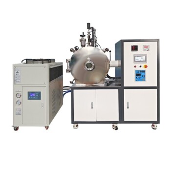
Lab-Scale Vacuum Induction Melting Furnace
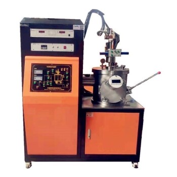
Non Consumable Vacuum Arc Induction Melting Furnace
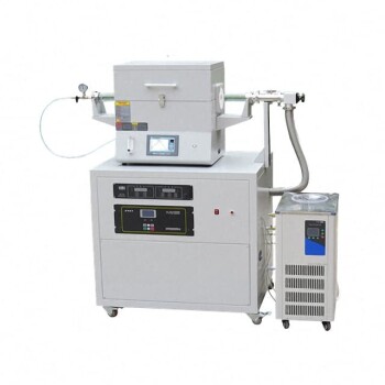
Split Chamber CVD Tube Furnace with Vacuum Station Chemical Vapor Deposition System Equipment Machine
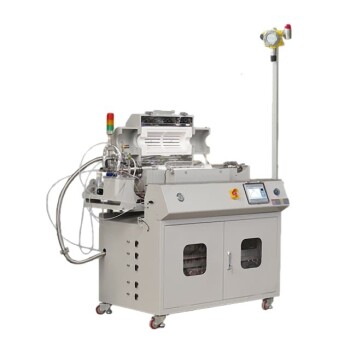
Customer Made Versatile CVD Tube Furnace Chemical Vapor Deposition Chamber System Equipment
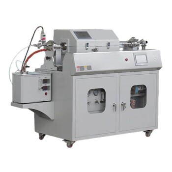
Chemical Vapor Deposition CVD Equipment System Chamber Slide PECVD Tube Furnace with Liquid Gasifier PECVD Machine
