Copper and nickel are widely regarded as the superior substrates for the Chemical Vapor Deposition (CVD) of graphene. While copper is the gold standard for producing exclusive graphene monolayers, nickel is highly effective for synthesizing structures with controlled layers.
These metals are favored not just for their chemical properties, but for their profound efficiency, cost-effectiveness, and the feasibility of scaling production to large dimensions.
Core Insight: The choice of substrate dictates the quality and thickness of the final material. Copper and nickel act as essential catalysts that lower reaction energy barriers, enabling the scalable production of high-quality, transferable graphene sheets suitable for high-performance electronics.
The Catalytic Role of the Substrate
To understand why specific metals are chosen, one must understand the function of the substrate in the CVD process.
Lowering Energy Barriers
In CVD, the metal substrate acts as a catalyst. It lowers the energy barrier required for the chemical reaction, facilitating the decomposition of feed materials (like methane) into carbon.
Determining Deposition Mechanisms
The substrate determines the specific mechanism of how carbon atoms assemble. This directly dictates the quality, uniformity, and layer count of the final graphene product.
Why Copper is Superior for Monolayers
Copper (Cu) is frequently cited as the premier choice for many applications, particularly in electronics.
Exclusive Monolayer Growth
The primary advantage of copper is its self-limiting nature regarding carbon absorption. It allows graphene to be deposited as exclusive monolayers.
High Homogeneity
Copper substrates typically yield graphene with high homogeneity and a low defect count. This makes them ideal for applications requiring high-performance, single-layer sheets.
The Utility of Nickel Substrates
While copper excels at monolayers, nickel (Ni) offers a different set of advantages for specific requirements.
Controlled Layer Formation
Nickel surfaces are effective for supporting the formation of controlled graphene layers.
Thicker Growth Potential
Because nickel interacts differently with carbon than copper does, it is often preferred when the goal is to create multi-layer graphene structures rather than strictly single atomic layers.
Key Operational Advantages
Beyond the chemical mechanics, copper and nickel are favored for practical manufacturing reasons.
Scalability to Large Dimensions
CVD on these transition metals is the most efficient method for preparing graphene with a huge surface area. This scalability is essential for moving from research labs to industrial commercialization.
Transferability
A critical feature of these substrates is that they can be etched away. This allows the graphene film to be transferred onto other functional substrates, such as silicon dioxide, for integration into devices.
Economic Viability
Both copper and nickel offer a balance of high quality and relative low cost. The process is cost-effective enough for mass production while maintaining the purity required for high-end applications.
Understanding the Trade-offs
While CVD on metal substrates is the leading approach, it is important to recognize the inherent complexities of the process.
The Transfer Requirement
Because the graphene is grown on a metal catalyst, it must be removed to be useful in electronics. This requires an etching process to dissolve the metal, which adds a step to the manufacturing workflow compared to direct-growth methods.
Cost vs. Quality
CVD is more expensive than methods used to produce lower-quality graphene (such as powders). However, for high-performance electronics and sensors where low defect counts and high purity are non-negotiable, the cost is justified.
Making the Right Choice for Your Goal
Selecting between copper and nickel depends entirely on the specific requirements of your end application.
- If your primary focus is single-layer precision: Choose copper, as it naturally limits deposition to exclusive monolayers with high homogeneity.
- If your primary focus is multi-layer structures: Choose nickel, as it supports the formation of controlled, multiple graphene layers effectively.
- If your primary focus is industrial scalability: Both metals are suitable, offering the best balance of large-area synthesis and cost-efficiency.
Ultimately, metal-substrate CVD remains the most effective method available for acquiring high-quality graphene for technological applications.
Summary Table:
| Substrate Property | Copper (Cu) | Nickel (Ni) |
|---|---|---|
| Graphene Layers | Exclusive Monolayers | Controlled Multi-layers |
| Growth Mechanism | Self-limiting surface growth | Carbon segregation/precipitation |
| Homogeneity | Very High | Variable (layer dependent) |
| Primary Application | High-end electronics & sensors | Multi-layer graphene structures |
| Scalability | High (Large-area) | High (Large-area) |
| Transferability | Easy (via metal etching) | Easy (via metal etching) |
Advance Your Material Research with KINTEK Precision
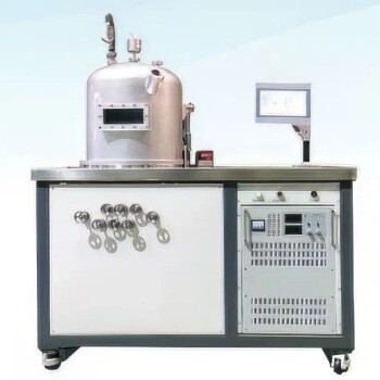
Unlock the full potential of your graphene synthesis with KINTEK’s industry-leading laboratory solutions. Whether you are aiming for exclusive monolayer homogeneity on copper or controlled multi-layer growth on nickel, our advanced CVD systems and high-temperature furnaces provide the thermal stability and precision required for superior results.
From high-performance CVD and PECVD systems to essential high-purity consumables and transfer tools, KINTEK specializes in equipping researchers and industrial manufacturers with the tools to scale innovation. Contact us today to discuss your project requirements and see how our expertise in laboratory equipment can streamline your path to high-quality graphene production.
Related Products
- Laboratory CVD Boron Doped Diamond Materials
- Custom CVD Diamond Coating for Lab Applications
- MgF2 Magnesium Fluoride Crystal Substrate Window for Optical Applications
- Carbon Graphite Plate Manufactured by Isostatic Pressing Method
- CVD Diamond for Thermal Management Applications
People Also Ask
- What are the applications of CVD diamonds? From Jewelry to High-Tech Tools
- What is the purpose of adding a boron source in CVD diamond growth? Master P-Type Semiconductor Conductivity
- How much cheaper are CVD diamonds? Save 20-30% on a Genuine Diamond
- What materials are CVD deposition? From Semiconductors to Super-Hard Coatings
- Do CVD diamonds pass diamond tester? Yes, they are real diamonds.
