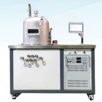
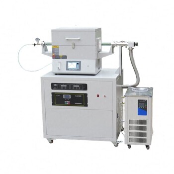
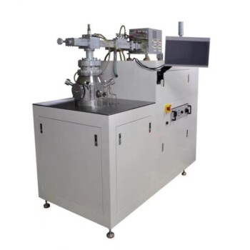
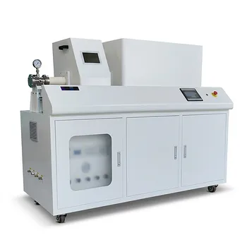
Chemical Vapor Deposition (CVD) is considered an efficient technique primarily for the fabrication of high-purity, high-performance thin solid films. It is specifically regarded as the definitive method for designing high-quality, large-area graphene thin films used in electronic transistors, corrosion coatings, and transparent conductors.
Core Takeaway: CVD provides a unique combination of scalability and precision, enabling the rapid production of uniform coatings on complex, irregular surfaces without the need for ultra-high vacuum environments.
The Primary Applications of CVD
While CVD is a versatile tool in manufacturing, its efficiency is best realized in specific high-value applications where film quality and uniformity are paramount.
Advanced Electronics and Graphene
According to the primary technical consensus, CVD is the most efficient technique for fabricating large-area graphene thin films. This is critical for modern electronics, particularly in the creation of electronic transistors and transparent conductors where material purity dictates performance.
Semiconductor Fabrication
CVD is standard practice for depositing thin films on semiconductors. Its ability to create layers with both organic and inorganic compounds makes it indispensable in the production of integrated circuits.
Energy and Industrial Tooling
In the solar energy sector, CVD is used to manufacture thin-film solar cells by depositing photovoltaic materials onto substrates. In heavy industry, it applies wear-resistant and thermal barrier coatings to cutting tools, significantly extending their operational lifespan.
Why CVD is Considered "Efficient"
To understand why professionals choose CVD over alternatives like Physical Vapor Deposition (PVD), you must look at the mechanical advantages of the process.
Non-Line-of-Sight Deposition
Unlike PVD, CVD is not limited to "line-of-sight" application. It possesses high "throwing power," meaning it can coat holes, deep recesses, and complex contoured surfaces with uniform thickness. This is essential for irregularly shaped substrates.
High Scalability and Speed
CVD offers high deposition rates, making it a high-speed process suitable for mass production. It allows for large-area deposition, which is a key factor in its cost-effectiveness relative to slower, more limited coating methods.
Cost and Environment
The process is relatively low-cost because it typically does not require an ultra-high vacuum. Furthermore, it eliminates the need for many extra side materials, streamlining the production line.
Understanding the Operational Factors
While efficient, CVD operates under specific conditions that dictate its suitability for a project.
Thermal Requirements
The process generally utilizes high reaction temperatures. While this allows for the use of diverse pre-materials, it requires substrates that can withstand significant thermal stress.
Chemical Complexity
CVD involves mixing source materials with volatile precursors. This relies on chemical reactions at the molecular level to achieve nucleation and growth, rather than simple physical deposition. This chemistry is what allows for the control of film porosity and crystalline structure.
Making the Right Choice for Your Project
CVD is a powerful technique, but it should be selected based on your specific engineering goals.
- If your primary focus is Graphene or 2D Materials: CVD is the superior choice for generating high-quality, large-area films for transistors and conductors.
- If your primary focus is Complex Geometry: CVD is required if your part has deep holes, recesses, or irregular shapes that line-of-sight methods cannot reach.
- If your primary focus is Mass Production: CVD offers the high deposition speeds and large-area coverage necessary for scalable, cost-effective manufacturing.
CVD remains the industry standard where the requirement for high-purity, uniform coatings meets the need for industrial scalability.
Summary Table:
| Feature | Efficiency Benefit | Key Applications |
|---|---|---|
| Deposition Style | Non-line-of-sight (covers deep recesses/holes) | Complex tooling, irregular substrates |
| Material Quality | High purity and uniform crystalline structure | Graphene films, electronic transistors |
| Scalability | High deposition rates for large-area coverage | Solar cells, mass-produced semiconductors |
| Vacuum Needs | No ultra-high vacuum required | Cost-effective industrial manufacturing |
Elevate Your Material Science with KINTEK
Ready to harness the efficiency of Chemical Vapor Deposition for your next breakthrough? KINTEK specializes in providing world-class laboratory equipment tailored for precision and scalability. Whether you are developing high-quality graphene or advanced semiconductor components, our comprehensive range of CVD and PECVD systems ensures uniform, high-purity results every time.
From high-temperature furnaces and vacuum systems to essential consumables like ceramics and crucibles, KINTEK supports your entire research and production workflow. Experience the KINTEK advantage in precision engineering—Contact our experts today to find the perfect solution for your lab!
Related Products
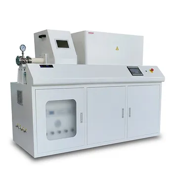
- Chemical Vapor Deposition CVD Equipment System Chamber Slide PECVD Tube Furnace with Liquid Gasifier PECVD Machine
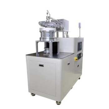
- Microwave Plasma Chemical Vapor Deposition MPCVD Machine System Reactor for Lab and Diamond Growth
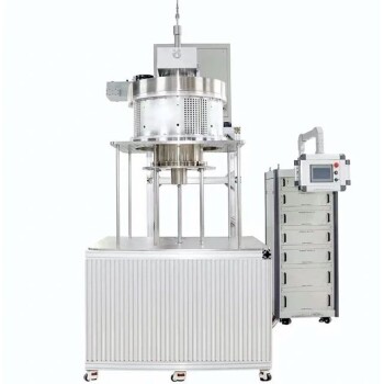
- 915MHz MPCVD Diamond Machine Microwave Plasma Chemical Vapor Deposition System Reactor
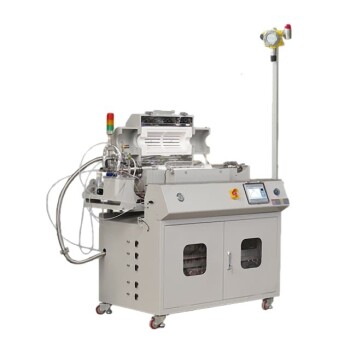
- Customer Made Versatile CVD Tube Furnace Chemical Vapor Deposition Chamber System Equipment
- HFCVD Machine System Equipment for Drawing Die Nano-Diamond Coating
People Also Ask
- How expensive is chemical vapor deposition? Understanding the True Cost of High-Performance Coating
- What is plasma enhanced chemical vapor deposition PECVD equipment? A Guide to Low-Temperature Thin Film Deposition
- How are carbon nanotubes grown? Master Scalable Production with Chemical Vapor Deposition
- What is the chemical vapor deposition growth process? Build Superior Thin Films from the Atom Up
- What are the processes of vapor phase deposition? Understand CVD vs. PVD for Superior Thin Films
