The primary source of contamination during Chemical Vapor Deposition (CVD) diamond growth is the interaction between the high-energy plasma and the growth chamber itself. The plasma, while necessary to activate the gases, can unintentionally etch internal components, releasing foreign materials like silicon and boron that are subsequently trapped within the growing diamond lattice.
Contamination in CVD growth is typically a byproduct of the hardware environment rather than the feed gases alone. High-energy plasma degrades reactor components—specifically silica windows and substrates—releasing impurities that compromise the diamond's purity.
The Mechanism of Contamination
Plasma-Induced Etching
The CVD process relies on generating a plasma—using microwave power, hot filaments, or arc discharges—to break down carbon and hydrogen gases.
While this creates the necessary chemistry for diamond growth, the plasma is highly aggressive. It physically attacks and etches the interior surfaces of the vacuum chamber.
Material Incorporation
Once materials are etched from the chamber walls or components, they become airborne species within the vacuum environment.
These liberated atoms do not simply vanish; they settle onto the substrate and are incorporated into the atomic structure of the growing diamond crystal.
Common Contaminants
Silicon
Silicon is the most frequent contaminant found in CVD diamonds.
Its primary source is the silica windows used for observing the process or admitting microwave energy. It can also originate from the silicon substrate on which the diamond is grown.
Boron
Boron is another critical impurity that can alter the properties of the diamond.
Even trace amounts of boron-containing species present in the chamber materials or background environment can be significant enough to contaminate the diamond.
Understanding the Trade-offs
Hardware Placement vs. Purity
To mitigate silicon contamination, operators often attempt to position silica windows far away from the substrate or remove them entirely.
However, moving or removing windows can complicate process monitoring and energy coupling, creating a trade-off between operational visibility and chemical purity.
Process Byproducts vs. Visual Quality
Beyond foreign elements like silicon, the CVD process itself often produces graphite and other non-diamond carbon phases.
This results in crystals with rough, graphitized edges and a distinct brown coloration. While not "contamination" from an external source, this structural impurity requires cutting and post-growth HPHT (High Pressure High Temperature) annealing to achieve a colorless state.
Making the Right Choice for Your Goal
To manage contamination effectively, you must balance hardware configuration with post-processing requirements.
- If your primary focus is high chemical purity: Prioritize reactor designs that minimize silica components or position them significantly away from the plasma zone to reduce silicon etching.
- If your primary focus is optical grade (colorless) diamond: Expect to utilize HPHT annealing after growth to correct the brown coloration caused by structural irregularities and non-diamond carbon.
Success in CVD growth requires treating the reactor chamber not just as a vessel, but as an active participant in the chemical process.
Summary Table:
| Contaminant Source | Mechanism | Primary Impurity | Impact on Diamond |
|---|---|---|---|
| Silica Windows | Plasma-induced etching | Silicon (Si) | Most common impurity; affects lattice structure |
| Reactor Hardware | Aggressive plasma interaction | Boron (B) & Metals | Alters electrical and chemical properties |
| Silicon Substrates | Direct etching/incorporation | Silicon (Si) | Higher concentrations of Si near growth base |
| Process Byproducts | Non-diamond carbon phases | Graphite | Causes brown coloration and rough edges |
Elevate Your Thin-Film Research with KINTEK
Don't let reactor impurities compromise your synthetic diamond quality. KINTEK specializes in high-performance laboratory equipment designed for precision material science. From advanced MPCVD and PECVD systems engineered to minimize contamination to High-Pressure High-Temperature (HPHT) reactors for post-growth annealing, we provide the tools you need to achieve optical-grade purity.
Whether you are a researcher in semiconductor physics or a laboratory developing industrial gemstones, our comprehensive portfolio of vacuum systems, high-temperature furnaces, and specialized consumables ensures consistent, high-yield results.
Ready to optimize your CVD process? Contact us today to find the perfect solution for your lab!
Related Products
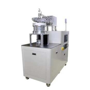
- Microwave Plasma Chemical Vapor Deposition MPCVD Machine System Reactor for Lab and Diamond Growth
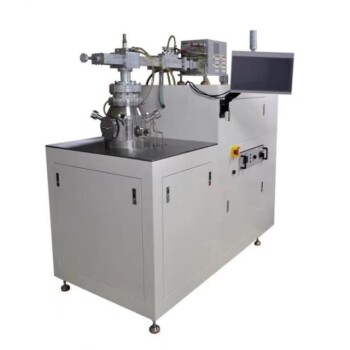
- Cylindrical Resonator MPCVD Machine System Reactor for Microwave Plasma Chemical Vapor Deposition and Lab Diamond Growth
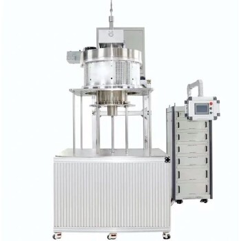
- 915MHz MPCVD Diamond Machine Microwave Plasma Chemical Vapor Deposition System Reactor
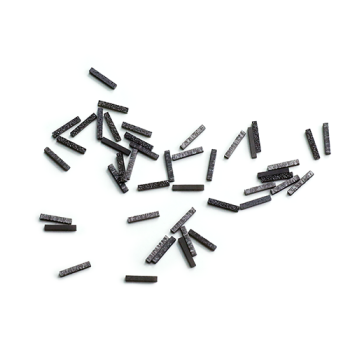
- CVD Diamond Dressing Tools for Precision Applications
- CVD Diamond Domes for Industrial and Scientific Applications
People Also Ask
- What pressure is needed for chemical vapor deposition of diamonds? Master the Low-Pressure 'Sweet Spot'
- What are the primary advantages of the CVD method for growing diamonds? Engineering High-Purity Gems and Components
- How does MPCVD work? A Guide to Low-Temperature, High-Quality Film Deposition
- Why is argon-rich gas phase chemistry used for UNCD growth? Unlock Precision Nano-Diamond Synthesis
- How does a microwave plasma reactor facilitate the synthesis of diamond? Master MPCVD with Precision Technology
