The future of Chemical Vapor Deposition (CVD) diamond is defined by two key frontiers: large-scale, high-purity single-crystal production and rapid expansion into advanced thermal management. These developments are pushing CVD diamond far beyond its use as a gemstone and into the core of next-generation electronics and industrial applications.
The evolution of CVD diamond is no longer about mimicking a natural gem. It's about engineering a superior material with unparalleled thermal and physical properties, positioning it as a critical enabler for high-performance technology.
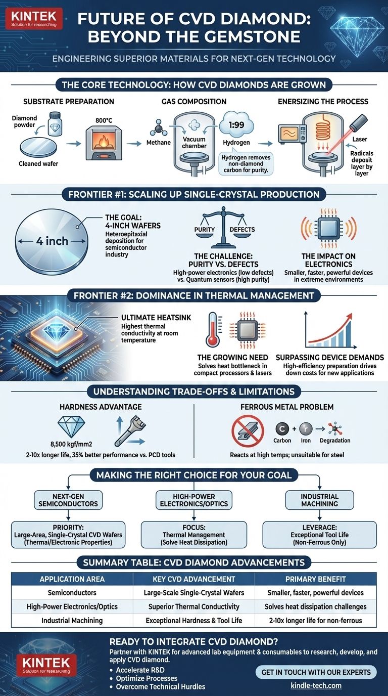
The Core Technology: How CVD Diamonds Are Grown
The Foundation: Substrate Preparation
The process begins with a substrate, which acts as the seed for diamond growth. The material choice and its crystallographic orientation are critical.
This substrate is meticulously cleaned, often with diamond powder, and heated to an optimal temperature of around 800°C (1,470°F) to prepare it for deposition.
The Building Blocks: Gas Composition
A mixture of gases is then introduced into a vacuum chamber. This typically consists of a carbon source, usually methane, and a much larger volume of hydrogen, often in a 1:99 ratio.
Hydrogen is essential. It performs the critical function of selectively etching away any non-diamond carbon that forms, ensuring a pure diamond structure grows.
The Catalyst: Energizing the Process
This gas mixture must be energized to create chemically active radicals that can deposit onto the substrate.
Common methods for this include using high-power microwaves, a hot filament, or a laser to break down the gases and initiate the growth process layer by layer.
Frontier #1: Scaling Up Single-Crystal Production
The Goal: 4-Inch Wafers
The primary goal is to master heteroepitaxial deposition, a technique for growing a high-quality crystal layer on a substrate of a different material. This is the key to producing large, 4-inch single-crystal diamond wafers.
Achieving this scale is a massive leap forward, making diamond a viable material for the semiconductor industry, which operates on standardized wafer sizes.
The Challenge: Purity vs. Defects
The central engineering challenge is balancing extreme purity with a low defect density. Different applications require a different balance.
For example, high-power electronics may prioritize defect-free structures for thermal conductivity, while quantum sensors might demand unparalleled purity to eliminate noise.
The Impact on Electronics
Successfully producing large-scale diamond wafers will enable the creation of smaller, faster, and more powerful electronic devices that can operate in extreme environments without overheating.
Frontier #2: Dominance in Thermal Management
Why Diamond is the Ultimate Heatsink
Diamond possesses the highest thermal conductivity of any known material at room temperature. This makes it exceptionally effective at drawing heat away from sensitive electronic components.
The Growing Need
As processors, lasers, and power electronics become more compact and powerful, they generate an immense amount of waste heat. This heat is often the primary limiting factor in their performance and reliability.
CVD diamond provides a solution to this critical bottleneck, enabling technologies to operate at their full potential without thermal failure.
Surpassing Device Demands
Advancements in high-efficiency CVD preparation are happening so quickly that the ability to produce diamond heat sinks may soon surpass the immediate demands of device manufacturers.
This surplus capacity will likely drive down costs and open up entirely new applications where thermal management was previously thought to be too expensive.
Understanding the Trade-offs and Limitations
The Hardness Advantage
CVD diamond is exceptionally hard, with a hardness of 8,500 kgf/mm2. This makes it a superior material for cutting tools.
Compared to Polycrystalline Diamond (PCD) tools, CVD tools can have a life 2 to 10 times longer and offer approximately 35% better performance in the right applications.
The Ferrous Metal Problem
Despite its hardness, CVD diamond is not suitable for machining steel or other ferrous alloys.
At the high temperatures generated during cutting, the carbon in the diamond reacts with the iron in the steel, causing the tool to rapidly degrade and wear out. It is best suited for non-ferrous materials like aluminum alloys, composites, and ceramics.
Making the Right Choice for Your Goal
The application of these advancements depends entirely on your primary engineering goal.
- If your primary focus is next-generation semiconductors: Prioritize developments in large-area, single-crystal CVD wafers for their superior thermal and electronic properties.
- If your primary focus is high-power electronics or optics: Focus on CVD diamond's thermal management capabilities to solve critical heat dissipation challenges that limit performance.
- If your primary focus is industrial machining: Leverage CVD's exceptional tool life for non-ferrous materials, but remain aware of its chemical limitations with steel.
Ultimately, CVD diamond is transitioning from a specialized material into a foundational component for future technological progress.
Summary Table:
| Application Area | Key CVD Diamond Advancement | Primary Benefit |
|---|---|---|
| Semiconductors | Large-Scale Single-Crystal Wafers | Enables smaller, faster, more powerful devices |
| High-Power Electronics / Optics | Superior Thermal Conductivity | Solves critical heat dissipation challenges |
| Industrial Machining | Exceptional Hardness & Tool Life | 2-10x longer life for non-ferrous materials |
Ready to Integrate CVD Diamond into Your Next Project?
As CVD diamond evolves from a specialized material to a foundational technology, partnering with the right equipment supplier is crucial. KINTEK specializes in providing the advanced lab equipment and consumables needed to research, develop, and apply CVD diamond for semiconductors, thermal management, and industrial machining.
Our expertise can help you:
- Accelerate R&D with precise and reliable deposition systems.
- Optimize Processes for high-purity, low-defect diamond growth.
- Overcome Technical Hurdles in scaling production for your specific application.
Contact us today to discuss how our solutions can empower your next breakthrough with CVD diamond technology.
Visual Guide
Related Products
- CVD Diamond for Thermal Management Applications
- CVD Diamond Optical Windows for Lab Applications
- CVD Diamond Domes for Industrial and Scientific Applications
- CVD Diamond Dressing Tools for Precision Applications
- Custom CVD Diamond Coating for Lab Applications
People Also Ask
- What is the chemical vapour deposition method for diamonds? Grow a Diamond from a Gas
- How long does it take to grow a CVD diamond? A 2-4 Week Journey to a Flawless Gem
- What are the characteristics of CVD diamond? Unlocking Superior Performance for Industrial Tools
- What are the optical properties of CVD diamond? Unlock Unmatched Performance for Demanding Applications
- Will a CVD diamond pass a diamond tester? Yes, because it's a real diamond.