CVD-grown graphene is currently deployed across a spectrum of high-performance technologies, ranging from advanced computing to renewable energy. Its primary modern applications include the design of heterostructures with semiconductors, nonvolatile memory storage, optoelectronics, and thermal management systems.
The Core Utility While graphene has many theoretical uses, CVD (Chemical Vapor Deposition) specifically enables the creation of high-purity, large-area films. This makes it the standard choice for transparent electrodes and active layers where optical transparency must coexist with high electrical conductivity.
Advancing Electronic Architecture
CVD graphene is not just a standalone material; it is a critical building block for next-generation component architecture.
Heterostructure Design
A primary application is the creation of heterostructures. Engineers stack CVD graphene with traditional semiconductors and other two-dimensional materials to create novel electronic components with tailored properties.
Nonvolatile Memories
In the storage sector, CVD graphene is being integrated into nonvolatile memory devices. Its stability and conductivity allow for data retention without constant power, a critical requirement for modern computing.
Interconnections and FETs
CVD graphene serves as a material for interconnections within integrated circuits. Additionally, its high carrier mobility makes it a prime candidate for the fabrication of Field-Effect Transistors (FETs), potentially surpassing the limitations of silicon in specific switching applications.
Optoelectronics and Energy
The material's unique combination of transparency and conductivity drives its adoption in light-based technologies.
Transparent Electrodes
CVD graphene is a superior alternative to traditional materials for transparent conductive films. With sheet resistance around 350 Ω/sq and optical transparency of roughly 90%, it is ideal for organic electronic devices.
Solar Cells
The material is actively used as an electrode in both organic (OPV) and inorganic (silicon) solar cells. It functions effectively as both a transparent electrode and an active layer, facilitating efficient photon harvesting.
Light-Emitting Diodes (LEDs)
Beyond harvesting energy, CVD graphene is used in light emission. It serves as a key component in high-performance LEDs and photodetectors, leveraging its ability to transmit light while conducting current.
Specialized Sensing and Mechanics
Modern applications extend into niche fields requiring durability and sensitivity at the nanoscale.
Bioelectronics
Due to its biocompatibility and electrical sensitivity, CVD graphene is increasingly used in bioelectronics. It acts as an interface between biological systems and electronic devices, enabling advanced monitoring and stimulation.
Thermal Management
Heat dissipation is a major bottleneck in electronics. CVD graphene is utilized in thermal management solutions to efficiently spread and dissipate heat, protecting sensitive components from thermal throttling.
Nanomechanical Systems
The material's exceptional strength-to-weight ratio allows it to be employed in nanomechanical systems, where it functions as a structural element that does not compromise weight or volume.
Thermo-electrochromic Sensors
Specific sensor applications include thermo-electrochromic sensors, where graphene serves as a core component for detecting temperature and electrical changes simultaneously.
Understanding the Trade-offs
While CVD graphene offers high performance, the production process involves specific technical challenges that dictate its quality.
Nucleation Density
Achieving large, continuous crystals is difficult. To produce millimeter-sized single-crystal flakes, engineers must conduct reactions above the melting point of copper to reduce nucleation density. High nucleation density leads to more grain boundaries, which can degrade electrical performance.
Substrate Management
The quality of the final graphene sheet is heavily dependent on the copper substrate. Issues such as the evaporation loss of copper during growth can introduce defects. Successful application requires precise control over the copper enclosure and the carbon source to maintain film integrity.
Making the Right Choice for Your Project
CVD graphene is versatile, but its application should align with your specific performance metrics.
- If your primary focus is Optoelectronics: Prioritize CVD graphene for its 90% transparency and low resistance, specifically for replacing brittle indium tin oxide (ITO) in solar cells or touchscreens.
- If your primary focus is Next-Gen Computing: Leverage its ability to form heterostructures with semiconductors to develop nonvolatile memory or advanced FETs.
- If your primary focus is Device Longevity: Utilize its thermal management properties to improve heat dissipation in densely packed microelectronic circuits.
CVD graphene represents the transition of 2D materials from theoretical physics to practical, high-performance industrial components.
Summary Table:
| Application Field | Key Component / Use Case | Primary Benefit |
|---|---|---|
| Electronics | FETs & Nonvolatile Memory | High carrier mobility & stable data retention |
| Optoelectronics | Transparent Electrodes | 90% optical transparency & 350 Ω/sq resistance |
| Energy | Solar Cells (OPV/Silicon) | Efficient photon harvesting & flexible conductivity |
| Thermal Management | Heat Spreaders | Superior heat dissipation for microelectronics |
| Bioelectronics | Biosensors & Interfaces | Biocompatibility & high electrical sensitivity |
| Mechanics | Nanomechanical Systems | Exceptional strength-to-weight ratio |
Unlock the Potential of 2D Materials with KINTEK
Ready to integrate high-performance CVD graphene into your next breakthrough? KINTEK specializes in providing the precision laboratory equipment and consumables essential for advanced material research and production. Whether you are developing next-generation semiconductors, solar cells, or bioelectronic interfaces, our comprehensive range of CVD and PECVD systems, high-temperature furnaces, and specialized ceramics ensures you achieve the high-purity results your project demands.
From crushing and milling systems for raw material preparation to sophisticated cooling solutions for sensitive experiments, KINTEK supports every stage of your lab's workflow. Contact us today to discover how our expertise in laboratory hardware and high-pressure reactors can elevate your research efficiency and material quality.
Related Products
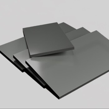
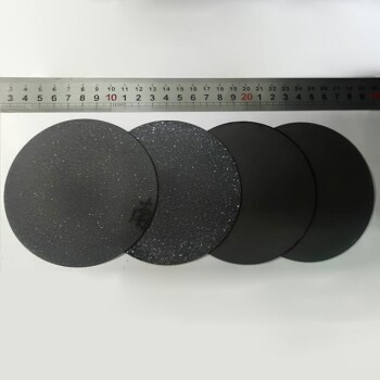
- Carbon Graphite Plate Manufactured by Isostatic Pressing Method
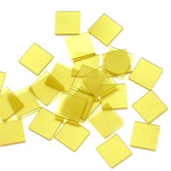
- Laboratory CVD Boron Doped Diamond Materials
- CVD Diamond for Thermal Management Applications
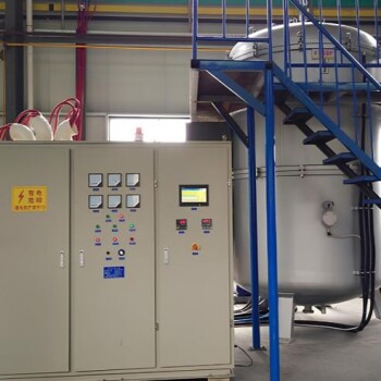
- Large Vertical Graphite Vacuum Graphitization Furnace
- Custom CVD Diamond Coating for Lab Applications
People Also Ask
- What is the density of isostatic graphite? Unlock Superior Performance for Demanding Applications
- What is isostatic pressing in powder metallurgy? Unlock Superior Part Density and Complexity
- What is isostatic pressing? Achieve Uniform Density and Complex Shapes
- What is the process of isostatic graphite manufacturing? Achieve Unmatched Material Uniformity and Performance
- What is isostatic graphite? The Ultimate Material for High-Tech and High-Temperature Applications
