MW-SWP CVD is preferred because it generates a "soft" plasma environment characterized by exceptionally low plasma potential. Unlike traditional inductive or capacitive coupled Radio Frequency (RF) discharge plasmas, which subject the growth surface to high-energy ion bombardment, Microwave Surface Wave Plasma Chemical Vapor Deposition (MW-SWP CVD) drastically reduces the kinetic energy of ions hitting the substrate. This prevents physical damage to the delicate atomic structure of the graphene during synthesis.
Core Takeaway The definitive advantage of MW-SWP CVD is the minimization of ion impact energy. By maintaining a low plasma potential, this method enables the synthesis of atomic-level thin films with superior crystalline quality, avoiding the structural defects caused by the aggressive ion bombardment inherent in traditional RF plasma systems.
The Mechanics of Plasma Damage
The Problem with Traditional RF Plasma
Traditional inductive or capacitive coupled RF discharge plasmas are effective for many coating applications, but they present a specific hazard for 2D materials. These systems typically operate with higher plasma potentials.
This high potential creates a strong electric field sheath near the substrate. Consequently, positive ions are accelerated toward the film surface with significant kinetic energy.
The Vulnerability of Graphene
Graphene is a single-atom-thick sheet of carbon. Because it lacks bulk volume to absorb impact, it is hypersensitive to physical forces.
High-energy ion bombardment acts like microscopic sandblasting on the growing film. This process introduces vacancies, tears, and structural disorders that destroy the material's unique electronic properties.
The MW-SWP Advantage
Low Plasma Potential
MW-SWP CVD distinguishes itself by creating a "soft plasma." The primary technical characteristic of this environment is its low electron temperature and, crucially, its low plasma potential.
Because the potential difference between the plasma and the substrate is minimal, ions are not accelerated to damaging speeds. They arrive at the surface with just enough energy to facilitate chemical reactions, but not enough to displace atoms.
Superior Crystalline Quality
The reduction in impact forces directly correlates to the quality of the final material. MW-SWP CVD allows the carbon atoms to arrange themselves into a hexagonal lattice with minimal disruption.
This results in non-destructive synthesis. The graphene sheets produced exhibit higher crystallinity and significantly fewer defects compared to those grown in high-impact RF environments.
Understanding the Context and Trade-offs
Application Suitability
While MW-SWP offers superior quality for delicate films, it is a specialized tool. It is engineered specifically to solve the problem of lattice damage in atomic-scale materials.
For robust, thick coatings where surface roughness or minor defects are acceptable, traditional RF methods may still be sufficient. However, for high-performance electronics where every atom counts, the "soft" nature of MW-SWP is a technical necessity, not just an alternative.
Making the Right Choice for Your Goal
To determine if MW-SWP CVD is the required approach for your specific project, consider your performance targets:
- If your primary focus is high-performance electronics or sensors: You must prioritize MW-SWP CVD to ensure the low defect count and high uniformity required for reliable electron transport.
- If your primary focus is synthesizing delicate 2D materials (like hBN or Graphene): You should utilize MW-SWP to prevent ion bombardment from compromising the structural integrity of the atomic lattice.
MW-SWP CVD effectively bridges the gap between plasma-enhanced synthesis and the preservation of atomic perfection.
Summary Table:
| Feature | Traditional RF Plasma (Inductive/Capacitive) | MW-SWP CVD (Microwave Surface Wave) |
|---|---|---|
| Plasma Environment | "Hard" plasma with high energy | "Soft" plasma with low potential |
| Ion Bombardment | High-energy; aggressive impact | Low-energy; gentle arrival |
| Impact on Graphene | High defect count; vacancies and tears | Non-destructive; preserves lattice |
| Crystalline Quality | Lower due to structural disorder | Superior; high crystallinity |
| Primary Application | Robust, thick industrial coatings | High-performance 2D materials & electronics |
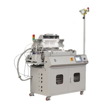
Precision matters when every atom counts. KINTEK provides state-of-the-art MW-SWP CVD systems, PECVD solutions, and high-temperature furnaces designed specifically for the synthesis of delicate 2D materials. Whether you are developing high-performance electronics or advanced sensors, our equipment ensures the structural integrity of your graphene and hBN films by minimizing ion damage. Enhance your research with our comprehensive range of high-pressure reactors, battery research tools, and laboratory consumables. Contact KINTEK today to optimize your synthesis process!
References
- Golap Kalita, Masayoshi Umeno. Synthesis of Graphene and Related Materials by Microwave-Excited Surface Wave Plasma CVD Methods. DOI: 10.3390/appliedchem2030012
This article is also based on technical information from Kintek Solution Knowledge Base .
Related Products
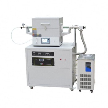
- Multi Heating Zones CVD Tube Furnace Machine Chemical Vapor Deposition Chamber System Equipment
- Split Chamber CVD Tube Furnace with Vacuum Station Chemical Vapor Deposition System Equipment Machine
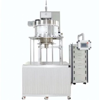
- 915MHz MPCVD Diamond Machine Microwave Plasma Chemical Vapor Deposition System Reactor
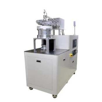
- Microwave Plasma Chemical Vapor Deposition MPCVD Machine System Reactor for Lab and Diamond Growth
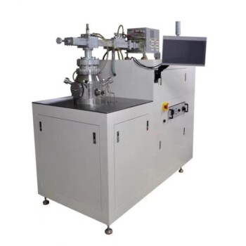
- Cylindrical Resonator MPCVD Machine System Reactor for Microwave Plasma Chemical Vapor Deposition and Lab Diamond Growth
People Also Ask
- What are the advantages of using a Multi-zone Tube Furnace? Enhanced Thermal Uniformity for Diffusion Research
- What is the difference between hot wall CVD and cold wall CVD? Choose the Right System for Your Process
- What is the function of a tube furnace in CVD SiC synthesis? Achieving Ultra-Pure Silicon Carbide Powders
- What is a CVD tube furnace? A Complete Guide to Thin-Film Deposition
- What are the advantages of a multi-zone tube furnace for Sb2S3? Unlock Superior Semiconductor Thin Film Purity

