Achieving perfect uniformity in Chemical Vapor Deposition (CVD) graphene is primarily hindered by kinetic transport dynamics. Within the reaction chamber, the gas flow is governed by complex forces of diffusion and convection that create variable conditions across the substrate. Because these fluid dynamics change as the gas moves, the chemical reactions responsible for graphene growth do not occur consistently from one end of the material to the other.
The root cause of non-uniformity lies in the changing availability of reactants across the substrate. Fluid dynamics cause gas concentrations to drop as they travel, preventing the consistent chemical reactions necessary for a perfectly even layer.
The Role of Gas Transport Dynamics
The Impact of Diffusion and Convection
The fundamental challenge is that the gas environment inside a CVD chamber is never static.
Diffusion and convection constantly alter how the gas moves and interacts with the substrate surface.
This dynamic movement means that the local environment at one specific point on the substrate may differ drastically from a point just a few centimeters away.
Reactant Depletion
As the precursor gas flows across the substrate, it is consumed by the reaction process.
By the time the gas reaches the far ends of the substrate, the concentration of reactants is often significantly lower than at the entry point.
This phenomenon, known as reactant depletion, makes it physically difficult to sustain the same rate of growth across the entire surface area.
The Complexity of Growth Variables
Multiplicity of Conditions
Beyond fluid dynamics, uniformity is threatened by a vast array of interconnected physical conditions.
Key variables such as surrounding pressure, temperature, and carrier gas composition must be perfectly synchronized.
Even the material of the reaction chamber itself plays a significant role in how these variables interact during the growth phase.
The Single-Layer Challenge
The difficulty spikes significantly when the goal is a pristine single-layer graphene film.
With so many variables in play, maintaining control over the quality and thickness of a layer that is only one atom thick requires exceptional precision.
Slight variances in the growth environment that might be negligible for bulk materials can completely disrupt the uniformity of a monolayer.
Common Pitfalls to Avoid
Overlooking Scalability Issues
It is a common pitfall to assume that a recipe working on a small sample will translate to a larger substrate.
The depletion effect described earlier becomes exponentially more difficult to manage as the surface area of the substrate increases.
Ignoring Component Interaction
Focusing solely on gas flow while ignoring temperature gradients is a mistake.
The fluid dynamics are thermally driven; therefore, inconsistencies in the heater or chamber insulation will exacerbate the kinetic transport issues, compounding the non-uniformity.
Approaches to Improve Uniformity
While the physics of CVD make uniformity difficult, specific strategies can mitigate these effects depending on your project goals.
- If your primary focus is maximizing uniformity: Consider modifying the concentration of gases to compensate for downstream depletion or incorporating spin coating methods to assist distribution.
- If your primary focus is optical quality: strictly control the pressure and temperature variables, as these dictate the transparency and sheet resistance of the final film.
Mastering CVD graphene growth requires viewing the reaction chamber not as a static oven, but as a dynamic fluid system where gas transport dictates the final material quality.
Summary Table:
| Challenge Factor | Impact on Graphene Uniformity | Recommended Mitigation Strategy |
|---|---|---|
| Gas Transport Dynamics | Diffusion and convection create inconsistent reaction conditions. | Optimize chamber fluid dynamics and gas flow rates. |
| Reactant Depletion | Gas concentration drops as it moves across the substrate. | Adjust precursor concentrations to compensate for downstream loss. |
| Variable Synchronization | Pressure, temperature, and carrier gas must be perfectly balanced. | Utilize precise temperature controllers and pressure regulators. |
| Scaling Issues | Uniformity becomes exponentially harder as substrate size increases. | Redesign chamber geometry for larger surface area coverage. |
Elevate Your Graphene Research with KINTEK Precision
Achieving atomic-level uniformity in CVD graphene requires more than just a recipe—it demands high-precision hardware designed for complex fluid dynamics. KINTEK specializes in advanced laboratory solutions tailored for the most demanding material science applications.
Whether you are tackling reactant depletion in CVD and PECVD systems or require reliable high-temperature furnaces and vacuum solutions, our expert-engineered equipment ensures the stability and control necessary for perfect thin-film deposition. From high-pressure reactors to crucibles and specialized ceramics, we provide the tools that turn laboratory challenges into scalable breakthroughs.
Ready to master your CVD process? Contact our technical experts today to find the ideal equipment for your research goals.
Related Products
- CVD Diamond Dressing Tools for Precision Applications
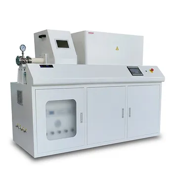
- Multi Heating Zones CVD Tube Furnace Machine Chemical Vapor Deposition Chamber System Equipment
- CVD Diamond Domes for Industrial and Scientific Applications
- CVD Diamond for Thermal Management Applications
- Chemical Vapor Deposition CVD Equipment System Chamber Slide PECVD Tube Furnace with Liquid Gasifier PECVD Machine
People Also Ask
- What is chemical vapor deposition of diamond? Grow High-Purity Diamonds Atom-by-Atom
- What are the disadvantages of CVD diamonds? Understanding the trade-offs for your purchase.
- What are the raw materials for CVD diamonds? A seed, a gas, and the science of crystal growth.
- How do CVD diamonds grow? A Step-by-Step Guide to Lab-Grown Diamond Creation
- What color diamonds are CVD? Understanding the Process from Brown Tint to Colorless Beauty
