Chemical Vapor Deposition (CVD) is the premier technique for synthesizing high-quality, large-area graphene sheets. It functions by introducing gaseous reactants—typically carbon sources like methane—into a controlled chamber, where they decompose and deposit a thin film onto a targeted substrate.
Chemical Vapor Deposition stands out as the dominant method for creating high-purity, monolayer graphene on an industrial scale. While other methods exist, CVD is currently the only process capable of meeting the volume and surface-area requirements of commercial manufacturing.
The Mechanics of the Process
A "Bottom-Up" Approach
Unlike "top-down" methods that break apart graphite to find graphene, CVD builds the material from scratch. It synthesizes graphene atom by atom, allowing for precise control over the final structure.
The Critical Role of the Substrate
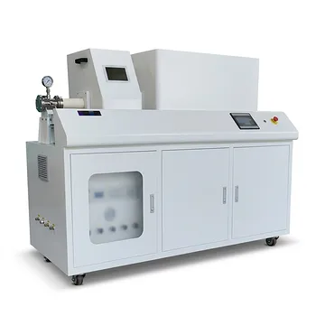
The process typically utilizes a transition metal substrate, most commonly copper (Cu) foil. This metal is placed in a tubular furnace and annealed (heated) in an atmosphere of hydrogen and argon to increase its grain size and prepare the surface.
Gas Decomposition and Deposition
Once the substrate is prepared, precursor gases containing carbon are introduced into the chamber. Under high heat, these gases decompose, leaving behind carbon atoms that settle onto the metal foil to form a continuous graphene film.
Why CVD is the Industry Standard
Unmatched Scalability
Since 2008, CVD has been recognized as the most successful method for scaling production. It is uniquely capable of fabricating graphene with a huge surface area, moving beyond microscopic flakes to sheets large enough for commercial electronics.
Superior Material Quality
CVD-grown graphene exhibits characteristics essential for high-performance applications. It offers high homogeneity, imperviousness, and high purity, with a fine grain structure that preserves the material's legendary electrical properties.
Control Over Layering
One of the distinct advantages of this method is the ability to control the number of layers produced. CVD is currently the most popular way to isolate graphene monolayers, which is critical for specific research and semiconductor applications.
Understanding the Trade-offs
Process Sensitivity
While efficient, the CVD process is delicate. The success of the deposition hinges on the rigorous monitoring and control of the substrate's temperature and gas transport kinetics.
The Transfer Challenge
Graphene grown via CVD is attached to a metal substrate (like copper) which is often not the final destination for the material. The metal must usually be etched away so the graphene film can be transferred to a functional substrate, such as silicon dioxide.
Cost vs. Quality Considerations
CVD is considered cost-effective for producing high-quality graphene. However, it remains more expensive than methods used to produce lower-quality graphene (such as powders or flakes), making it an investment reserved for applications where purity and sheet size are paramount.
Making the Right Choice for Your Goal
- If your primary focus is high-performance electronics: CVD is essential because it offers the homogeneity and monolayer control required for semiconductors and sensors.
- If your primary focus is industrial scalability: CVD is the best choice as it is the only current method capable of producing large-area sheets to meet mass demand.
- If your primary focus is absolute lowest cost: You may want to investigate other methods, as CVD carries a higher price tag than low-quality bulk production techniques.
CVD represents the critical bridge between theoretical graphene research and real-world, scalable application.
Summary Table:
| Feature | CVD Graphene Production Detail |
|---|---|
| Mechanism | Bottom-up synthesis (atom by atom) |
| Common Substrate | Copper (Cu) foil or Nickel (Ni) |
| Precursor Gas | Methane (CH4) or other hydrocarbons |
| Primary Output | Large-area, high-homogeneity monolayers |
| Key Applications | Semiconductors, high-performance electronics, and sensors |
| Scale | Industrial/Commercial manufacturing level |
Elevate Your Material Research with KINTEK Precision
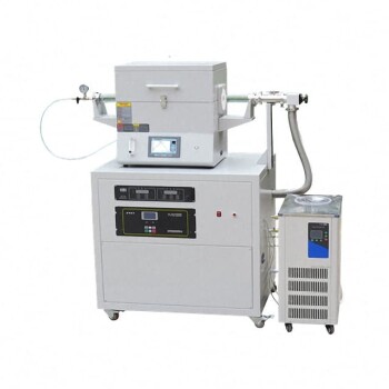
Transitioning from lab-scale discovery to industrial-scale production requires the highest standards of reliability. KINTEK specializes in advanced laboratory equipment, providing the cutting-edge CVD and PECVD systems, high-temperature tubular furnaces, and vacuum solutions essential for high-purity graphene synthesis.
Whether you are focusing on semiconductor development or large-area graphene sheets, our expertise in thermal processing and material science ensures you achieve unmatched homogeneity and control. Beyond CVD, we offer a comprehensive range of high-temperature reactors, crushing systems, and cooling solutions tailored for the most demanding research environments.
Ready to scale your production? Contact KINTEK today to discuss your project requirements!
Related Products
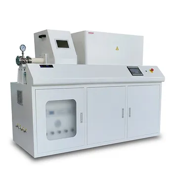
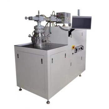
- Chemical Vapor Deposition CVD Equipment System Chamber Slide PECVD Tube Furnace with Liquid Gasifier PECVD Machine
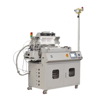
- Customer Made Versatile CVD Tube Furnace Chemical Vapor Deposition Chamber System Equipment
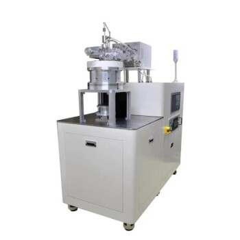
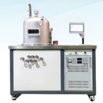
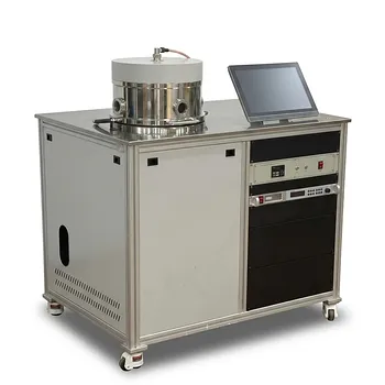
- Microwave Plasma Chemical Vapor Deposition MPCVD Machine System Reactor for Lab and Diamond Growth
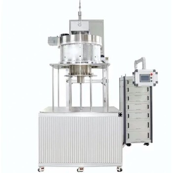
- 915MHz MPCVD Diamond Machine Microwave Plasma Chemical Vapor Deposition System Reactor
- Custom CVD Diamond Coating for Lab Applications
People Also Ask
- How are carbon nanotubes grown? Master Scalable Production with Chemical Vapor Deposition
- What is plasma enhanced chemical vapor deposition PECVD equipment? A Guide to Low-Temperature Thin Film Deposition
- What happens during deposition chemistry? Building Thin Films from Gaseous Precursors
- How expensive is chemical vapor deposition? Understanding the True Cost of High-Performance Coating
- Why is Chemical Vapor Deposition (CVD) equipment uniquely suited for constructing hierarchical superhydrophobic structures?
