Atomic Layer Chemical Vapour Deposition (ALCVD), also known as Atomic Layer Deposition (ALD), is a thin-film deposition technique valued for its ability to operate at lower growth temperatures while delivering exceptional film quality. Its primary benefits include producing coatings with superior uniformity and density, making it a critical process in modern semiconductor manufacturing.
The core value of ALCVD lies in its self-limiting nature, which allows for atomic-level control over film thickness. This precision enables the creation of defect-free, highly conformal coatings essential for the shrinking geometries of next-generation electronics.
The Mechanisms Behind the Benefits
Precision Through Self-Limiting Reactions
The defining characteristic of ALCVD is its self-limiting reaction mechanism. Unlike standard deposition methods that pile material continuously, ALCVD builds films one atomic layer at a time.
This sequential process ensures atomic layer thickness resolution. It grants you total control over the film’s composition and final thickness, eliminating the risk of over-deposition.
Superior Conformality on Complex Shapes
ALCVD is not a line-of-sight process because it utilizes gaseous reactants. This allows the gas to penetrate and coat restricted-access surfaces that other directional methods cannot reach.
Consequently, it achieves excellent conformality even on surfaces with high aspect ratios. Whether coating deep trenches or complex 3D structures, the film thickness remains uniform throughout.
High Purity and Structural Integrity
Films produced via ALCVD are characterized by low porosity and high density. The controlled reaction results in pinhole-free layers, which is vital for preventing electrical leakage in insulators.
Furthermore, the process yields films with high purity. Because the growth occurs at lower temperatures, it minimizes the risk of thermal damage to sensitive substrates while ensuring the film is fully crystallized.
Key Applications in Technology
Semiconductor Fabrication
ALCVD is the industry standard for creating critical components in microelectronics. It is specifically used to fabricate transistor gate dielectric layers, where insulation must be perfect at the nano-scale.
It is also widely utilized in forming metal gate electrodes. The ability to deposit dense, uniform metal layers without defects is crucial for the performance of modern logic devices.
Nanotechnology
Beyond standard chips, the technique is fundamental to nanotechnology applications. Its ability to coat fine holes and wrap around complex nanostructures allows for the engineering of advanced sensors and micro-electromechanical systems (MEMS).
Understanding the Trade-offs
Process Speed vs. Precision
While ALCVD offers unmatched quality, the layer-by-layer nature of the process can be inherently slower than bulk Chemical Vapour Deposition (CVD). You are trading rapid growth rates for atomic precision and uniformity.
Production Economics
Despite the slower growth rate per unit, the process can still be economical for mass production. This is because large batches of parts can often be coated simultaneously, balancing out the time required for the individual layers to form.
Making the Right Choice for Your Goal
When deciding if ALCVD is the correct method for your project, consider your specific constraints regarding geometry and tolerance.
- If your primary focus is extreme precision: ALCVD is the superior choice because it offers atomic-level thickness control and pinhole-free structural integrity.
- If your primary focus is complex geometry: Choose this method for its "throwing power," which ensures uniform coating on high aspect ratio structures and restricted surfaces.
ALCVD remains the definitive solution for applications where the margin for error is measured in atoms and film quality cannot be compromised.
Summary Table:
| Feature | ALCVD (ALD) Benefit | Application Impact |
|---|---|---|
| Thickness Control | Atomic-layer resolution | Enables defect-free coatings for next-gen electronics |
| Conformality | 100% step coverage | Ideal for high-aspect-ratio 3D structures and deep trenches |
| Film Quality | Low porosity & pinhole-free | Prevents electrical leakage in transistor gate dielectrics |
| Process Temp | Lower growth temperatures | Protects heat-sensitive substrates from thermal damage |
| Reaction Type | Self-limiting gaseous reaction | Ensures high purity and uniform composition across surfaces |
Elevate Your Material Research with KINTEK Precision
Ready to achieve atomic-level perfection in your deposition processes? KINTEK specializes in providing cutting-edge laboratory solutions, including high-performance CVD, PECVD, and MPCVD systems designed for the most demanding semiconductor and nanotechnology applications.
Beyond deposition, our comprehensive portfolio supports every stage of your workflow with high-temperature furnaces, high-pressure reactors, and precision crushing and milling systems. Partner with KINTEK for reliable equipment that guarantees uniformity, density, and structural integrity.
Maximize your lab's potential today—Contact our experts to find your custom solution!
Related Products
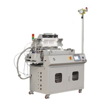
- Chemical Vapor Deposition CVD Equipment System Chamber Slide PECVD Tube Furnace with Liquid Gasifier PECVD Machine
- RF PECVD System Radio Frequency Plasma-Enhanced Chemical Vapor Deposition RF PECVD
- HFCVD Machine System Equipment for Drawing Die Nano-Diamond Coating
- 915MHz MPCVD Diamond Machine Microwave Plasma Chemical Vapor Deposition System Reactor
- Inclined Rotary Plasma Enhanced Chemical Vapor Deposition PECVD Equipment Tube Furnace Machine
People Also Ask
- How expensive is chemical vapor deposition? Understanding the True Cost of High-Performance Coating
- What happens during deposition chemistry? Building Thin Films from Gaseous Precursors
- What is the chemical vapor deposition growth process? Build Superior Thin Films from the Atom Up
- What are the core advantages of PE-CVD in OLED encapsulation? Protect Sensitive Layers with Low-Temp Film Deposition
- What are the advantages of chemical vapor deposition? Achieve Superior Thin Films for Your Lab
