Metal-organic Chemical Vapor Deposition (MOCVD) is a specialized deposition process that uses metal-organic compounds as precursors to form thin films on a substrate. These precursors, often vaporized liquids containing metal-carbon bonds, are introduced into a reaction chamber where they are thermally decomposed or activated by plasma or light. The metal center reacts to build the desired material layer, while the organic ligands are released and removed as byproducts.
The Core Insight: MOCVD is distinguished by its ability to offer precise control over film composition and doping levels. While standard CVD handles general materials, MOCVD is critical for fabricating the complex structures found in modern CMOS devices, such as compound semiconductors and high-quality dielectric films.
The Mechanics of MOCVD
The Role of Precursors
Unlike standard Chemical Vapor Deposition (CVD), which may use simple hydrides or halides, MOCVD relies specifically on metal-organic compounds. These molecules contain at least one chemical bond between a metal atom and a carbon atom.
The Reaction Process
Once these precursors enter the chamber, they undergo a specific transformation. The system applies energy—typically through thermal decomposition (heat), though plasma or light can also be used.
Selective Deposition
During this reaction, the chemical bonds break in a controlled manner. The metal center of the molecule deposits onto the wafer to form the film. Simultaneously, the organic components (ligands) are released as gaseous byproducts and exhausted from the chamber.
Applications in CMOS Fabrication
Compound Semiconductors
MOCVD is highly effective for depositing compound semiconductors (such as III-V materials). This capability allows for the growth of complex, multi-layered structures with varying compositions, which is essential for advanced transistor designs.
High-Quality Dielectric Films
In CMOS devices, insulating layers must be pristine to prevent electrical leakage. MOCVD is used to deposit high-quality dielectric films that serve as critical insulators between conductive layers.
Metal Films
The process is also utilized to deposit the metal films required for interconnects and contacts within the device. The precision of MOCVD ensures these metallic layers are uniform and conductive.
Understanding the Trade-offs
Managing Byproducts
A critical aspect of MOCVD is the release of organic ligands. Because the precursor contains carbon, the process must be strictly controlled to ensure these ligands are fully expelled as byproducts. Failure to do so can lead to unintentional carbon incorporation, potentially degrading the purity of the film.
Precursor Complexity
The use of metal-organic precursors adds a layer of complexity compared to simpler CVD methods. These precursors are often vaporized liquids, requiring precise delivery systems to maintain stable flow rates and accurate stoichiometry (chemical balance) in the final film.
Making the Right Choice for Your Goal
When evaluating deposition techniques for semiconductor projects, consider your specific requirements regarding material complexity and precision.
- If your primary focus is Compositional Control: MOCVD is the superior choice, allowing you to fine-tune doping levels and mix complex elements for compound semiconductors.
- If your primary focus is Advanced Dielectrics: MOCVD provides the high-quality, dense insulating films necessary for modern, scaled-down CMOS architectures.
MOCVD remains a cornerstone technology for delivering the material precision required by today's high-performance integrated circuits.
Summary Table:
| Feature | MOCVD Capability | CMOS Application Benefit |
|---|---|---|
| Precursor Type | Metal-organic compounds (metal-carbon bonds) | High purity & controlled chemical reactions |
| Material Range | III-V compound semiconductors & dielectrics | Essential for advanced multi-layer transistors |
| Control Level | Exceptional doping & composition control | Enables scaled-down, high-performance architectures |
| Film Quality | Uniform, dense, and high-quality films | Reliable insulation and high-conductivity interconnects |
Elevate Your Semiconductor Research with KINTEK
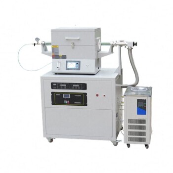
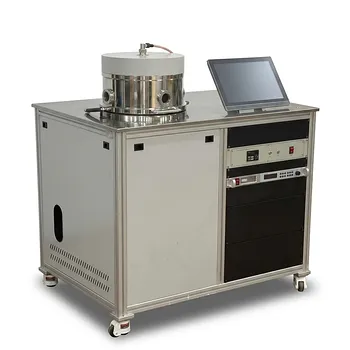
Unlock superior material precision for your next-generation CMOS devices. KINTEK specializes in high-performance laboratory equipment, providing the advanced solutions needed for complex deposition processes. From our specialized high-temperature furnaces (CVD, PECVD, MPCVD) and vacuum systems to precision crushing, milling, and hydraulic presses, we empower researchers to achieve flawless results.
Whether you are developing compound semiconductors or high-quality dielectric films, our comprehensive portfolio of consumables—including PTFE products, ceramics, and crucibles—ensures your lab operates at peak efficiency.
Ready to optimize your thin-film deposition? Contact our experts today to find the perfect equipment for your lab!
Related Products
- Multi Heating Zones CVD Tube Furnace Machine Chemical Vapor Deposition Chamber System Equipment
- Microwave Plasma Chemical Vapor Deposition MPCVD Machine System Reactor for Lab and Diamond Growth
- 915MHz MPCVD Diamond Machine Microwave Plasma Chemical Vapor Deposition System Reactor
- Cylindrical Resonator MPCVD Machine System Reactor for Microwave Plasma Chemical Vapor Deposition and Lab Diamond Growth
- Customer Made Versatile CVD Tube Furnace Chemical Vapor Deposition Chamber System Equipment
People Also Ask
- What is the difference between hot wall CVD and cold wall CVD? Choose the Right System for Your Process
- What advantages do CVD furnaces offer for Wf/W composites? Preserving Fiber Ductility and Interface Integrity
- What are the advantages of using a Multi-zone Tube Furnace? Enhanced Thermal Uniformity for Diffusion Research
- What are the advantages of a multi-zone tube furnace for Sb2S3? Unlock Superior Semiconductor Thin Film Purity
- How does a CVD tube furnace inhibit the sintering of silver supports? Boost Membrane Durability and Performance

