Vapour Phase Epitaxy (VPE) is a precise crystal growth technique used to manufacture high-quality semiconductor materials. It is a specialized form of Chemical Vapour Deposition (CVD) where a new thin layer is grown on a crystalline substrate, ensuring the new layer acts as a structural continuation of the substrate's original crystal orientation.
VPE distinguishes itself from standard deposition by maintaining a continuous single-crystal structure between the base and the new layer. This atomic alignment is critical for producing semiconductor devices that require high purity and specific electrical characteristics.
The Core Mechanism of VPE
Extending the Crystal Structure
The defining feature of VPE is epitaxy, which refers to the orderly growth of one crystal layer upon another.
Unlike standard coating methods that might deposit material randomly, VPE ensures the new atoms align perfectly with the lattice structure of the substrate.
This creates a seamless transition, allowing electrons to move efficiently through the material without being scattered by structural defects.
The Role of Chemical Vapour
As the name implies, the raw materials in VPE are introduced as vapours or gases.
These gases react chemically near or on the surface of the heated substrate.
The reaction deposits a solid film that adopts the exact geometric pattern of the underlying single crystal.
Methods and Material Quality
Common Processing Techniques
In the context of producing materials like Gallium Arsenide (GaAs), VPE typically utilizes one of two specific approaches:
- The Chloride Method
- The Hydride Method
These methods are tailored to manage the specific chemical precursors required to grow compound semiconductors.
Equipment and Purity
A significant advantage of VPE technology is the relative simplicity of the process equipment required compared to more complex growth methods.
Despite this simplicity, the method is capable of producing high-purity layers.
This high purity directly translates to superior electrical characteristics, making the material suitable for sensitive electronic applications.
Understanding the Trade-offs
Specificity of Application
VPE is highly specialized; it is not a general-purpose coating technique.
It is strictly designed for single-crystal growth, meaning it requires a high-quality single-crystal substrate to function correctly.
If the substrate has defects or an irregular surface, the epitaxial layer will likely replicate those flaws, potentially compromising the final device.
Applications in Electronics
Microwave and High-Frequency Devices
Because of its ability to produce high-purity GaAs, VPE is widely used in the manufacturing of microwave devices.
The method is instrumental in creating components that operate at high speeds and frequencies.
Key Components
Common devices fabricated using VPE-grown layers include:
- Field-Effect Transistors (FETs)
- Hall Devices (used for magnetic field sensing)
- Microwave Diodes (such as Gunn diodes)
Making the Right Choice for Your Project
VPE is a foundational technology for specific high-performance semiconductor needs.
- If your primary focus is material quality: VPE is ideal for generating high-purity single crystal layers with excellent electrical characteristics.
- If your primary focus is manufacturing efficiency: The process offers a balance of high performance with relatively simple process equipment compared to other epitaxial techniques.
VPE remains the method of choice when the crystal structure of the grown layer must perfectly match the substrate to ensure optimal device performance.
Summary Table:
| Feature | Vapour Phase Epitaxy (VPE) Details |
|---|---|
| Core Process | Specialized Chemical Vapour Deposition (CVD) |
| Growth Type | Epitaxial (Atomic alignment with substrate lattice) |
| Precursor State | Gaseous vapours (Chloride or Hydride methods) |
| Key Materials | Gallium Arsenide (GaAs), Compound Semiconductors |
| Main Applications | FETs, Microwave Diodes, Hall Devices |
| Primary Benefit | High purity with relatively simple equipment |
Elevate Your Semiconductor Research with KINTEK
Achieve unmatched material purity and crystal integrity with KINTEK’s advanced laboratory solutions. Whether you are scaling Vapour Phase Epitaxy (VPE) processes or developing next-generation microwave devices, we provide the precision tools your lab demands.
Our comprehensive portfolio supports every stage of semiconductor and materials research, including:
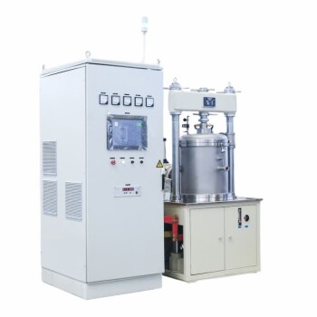
- High-Temperature Furnaces: CVD, Tube, and Atmosphere furnaces for precise epitaxial growth.
- Material Processing: Advanced crushing, milling, and hydraulic presses for substrate preparation.
- Vacuum & Thermal Control: High-performance vacuum systems and cooling solutions (ULT freezers, cold traps).
- Specialized Labware: High-purity ceramics, crucibles, and PTFE consumables.
Ready to optimize your thin-film deposition? Contact KINTEK today to discover how our high-performance equipment can streamline your workflow and ensure superior device performance.
Related Products
- Chemical Vapor Deposition CVD Equipment System Chamber Slide PECVD Tube Furnace with Liquid Gasifier PECVD Machine
- RF PECVD System Radio Frequency Plasma-Enhanced Chemical Vapor Deposition RF PECVD
- 915MHz MPCVD Diamond Machine Microwave Plasma Chemical Vapor Deposition System Reactor
- Inclined Rotary Plasma Enhanced Chemical Vapor Deposition PECVD Equipment Tube Furnace Machine
- Customer Made Versatile CVD Tube Furnace Chemical Vapor Deposition Chamber System Equipment
People Also Ask
- What are the advantages of chemical vapor deposition? Achieve Superior Thin Films for Your Lab
- What is plasma enhanced chemical vapor deposition PECVD equipment? A Guide to Low-Temperature Thin Film Deposition
- How expensive is chemical vapor deposition? Understanding the True Cost of High-Performance Coating
- What are the processes of vapor phase deposition? Understand CVD vs. PVD for Superior Thin Films
- What are the core advantages of PE-CVD in OLED encapsulation? Protect Sensitive Layers with Low-Temp Film Deposition