Knowledge cvd machine What is chemical vapor deposition in semiconductors? The Atomic-Scale Engine of Modern Electronics
Author avatar

Tech Team · Kintek Solution

Updated 2 months ago

What is chemical vapor deposition in semiconductors? The Atomic-Scale Engine of Modern Electronics


At its core, chemical vapor deposition (CVD) in semiconductors is a highly controlled process for building ultra-thin, solid films on top of a silicon wafer. It works by introducing specific gases into a reaction chamber, where they chemically react and deposit a layer of material, essentially constructing the microscopic components of a computer chip one atomic layer at a time.

CVD is not merely a coating technique; it is a fundamental fabrication method. It enables the construction of complex, multi-layered semiconductor devices by precisely transforming carefully selected gases into solid, functional films.

What is chemical vapor deposition in semiconductors? The Atomic-Scale Engine of Modern Electronics

How Chemical Vapor Deposition Works: The Core Mechanism

To understand CVD's importance, you must first understand its fundamental steps. The process is a carefully orchestrated sequence designed for atomic-level precision.

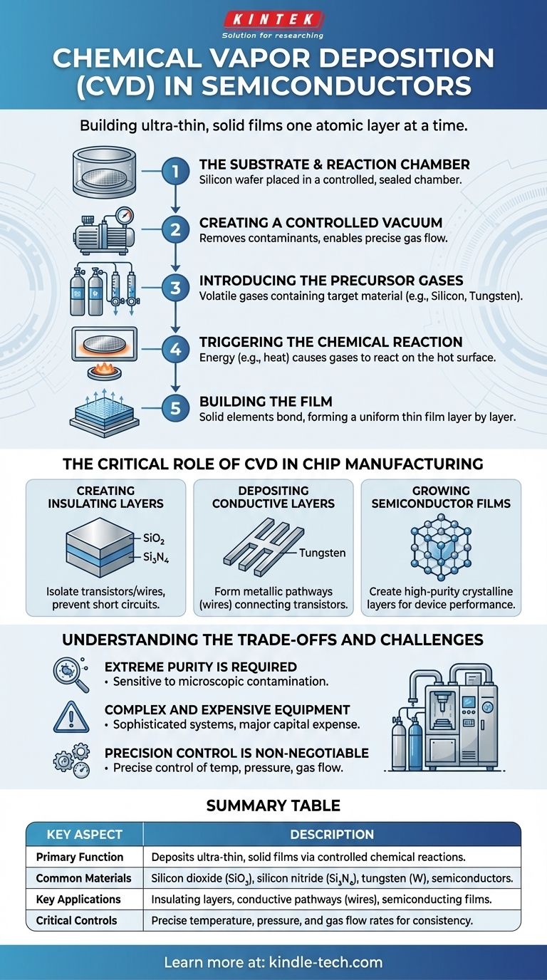
The Substrate and Reaction Chamber

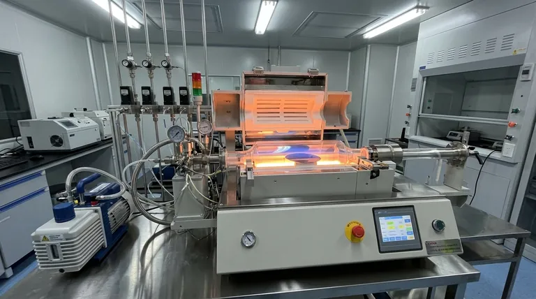
First, the workpiece—typically a silicon wafer—is placed inside a highly controlled, sealed reaction chamber. This chamber is engineered to maintain specific conditions of temperature and pressure.

Creating a Controlled Vacuum

The chamber is put under a vacuum. This step is critical for two reasons: it removes any unwanted atmospheric gases that could contaminate the film, and it allows for the precise control and flow of the reactive gases that will be introduced next.

Introducing the Precursor Gases

A specific mixture of volatile gases, known as precursors, is then introduced into the chamber. These gases contain the atoms of the material you want to deposit, such as silicon, nitrogen, or a metal like tungsten.

Triggering the Chemical Reaction

An energy source, most commonly heat, is applied to the chamber and the wafer. This energy causes the precursor gases to either break down or react with each other on the hot surface of the wafer.

Building the Film

As the gases react, the solid elements bond to the wafer's surface, forming a thin, uniform film. This process continues layer by layer, building the film to a precisely specified thickness across the entire wafer.

The Critical Role of CVD in Chip Manufacturing

CVD is not a single-use process; it's a versatile tool used repeatedly during chip fabrication to build different parts of the integrated circuit.

Creating Insulating Layers

One of the most common uses of CVD is to deposit films of silicon dioxide (SiO₂) or silicon nitride (Si₃N₄). These materials are excellent electrical insulators, used to isolate transistors and wires from each other to prevent short circuits.

Depositing Conductive Layers

CVD is also used to create the metallic pathways that connect the millions or billions of transistors on a chip. Films of materials like tungsten are deposited to act as the "wires" of the circuit.

Growing Semiconductor Films

The process can be used to grow the very semiconductor materials that form the transistors themselves. This allows for the creation of highly pure, crystalline layers with specific electronic properties essential for device performance.

Understanding the Trade-offs and Challenges

While powerful, CVD is a demanding and complex process that requires significant expertise and investment.

Extreme Purity is Required

The process is exceptionally sensitive to contamination. Even microscopic dust particles or trace amounts of unwanted gases can ruin the electronic properties of the deposited film, rendering the chip useless.

Complex and Expensive Equipment

CVD systems are highly sophisticated. They involve integrated gas delivery systems, high-temperature reaction chambers, powerful vacuum pumps, and automated control systems, making the equipment a major capital expense.

Precision Control is Non-Negotiable

The final quality and thickness of the deposited film depend on the precise control of variables like temperature, pressure, and gas flow rates. Maintaining this control consistently across an entire wafer requires a high level of process engineering skill.

How to Apply This to Your Goal

Understanding CVD is essential for anyone involved in electronics or materials science. Your perspective on it will depend on your specific focus.

  • If your primary focus is chip fabrication: Recognize CVD as a foundational "additive" manufacturing process, used to build up the critical insulating, conducting, and semiconducting layers of a microchip.
  • If your primary focus is materials science: View CVD as a versatile method for creating high-purity, high-performance thin films for a wide range of applications beyond semiconductors, including optics and protective coatings.
  • If your primary focus is process engineering: Concentrate on the critical control parameters—temperature, pressure, and gas chemistry—as these are the levers that determine a film's success or failure.

Ultimately, chemical vapor deposition is the invisible engine that enables the atomic-scale construction of the modern electronic world.

Summary Table:

Key Aspect Description
Primary Function Deposits ultra-thin, solid films on silicon wafers via controlled chemical reactions of gases.
Common Materials Silicon dioxide (SiO₂), silicon nitride (Si₃N₄), tungsten (W), and other semiconductors.
Key Applications Creating insulating layers, conductive pathways (wires), and semiconducting transistor films.
Critical Controls Precise temperature, pressure, and gas flow rates for consistent, high-quality results.

Ready to achieve precision in your lab's thin-film fabrication? KINTEK specializes in high-performance lab equipment and consumables, including solutions for demanding processes like CVD. Whether you're in R&D or production, our expertise ensures you have the reliable tools needed for superior results. Contact our specialists today to discuss how we can support your semiconductor or materials science projects.

Visual Guide

What is chemical vapor deposition in semiconductors? The Atomic-Scale Engine of Modern Electronics Visual Guide

Related Products

People Also Ask

Related Products

Chemical Vapor Deposition CVD Equipment System Chamber Slide PECVD Tube Furnace with Liquid Gasifier PECVD Machine

Chemical Vapor Deposition CVD Equipment System Chamber Slide PECVD Tube Furnace with Liquid Gasifier PECVD Machine

KT-PE12 Slide PECVD System: Wide power range, programmable temp control, fast heating/cooling with sliding system, MFC mass flow control & vacuum pump.

Microwave Plasma Chemical Vapor Deposition MPCVD Machine System Reactor for Lab and Diamond Growth

Microwave Plasma Chemical Vapor Deposition MPCVD Machine System Reactor for Lab and Diamond Growth

Get high-quality diamond films with our Bell-jar Resonator MPCVD machine designed for lab and diamond growth. Discover how Microwave Plasma Chemical Vapor Deposition works for growing diamonds using carbon gas and plasma.

915MHz MPCVD Diamond Machine Microwave Plasma Chemical Vapor Deposition System Reactor

915MHz MPCVD Diamond Machine Microwave Plasma Chemical Vapor Deposition System Reactor

915MHz MPCVD Diamond Machine and its multi-crystal effective growth, the maximum area can reach 8 inches, the maximum effective growth area of single crystal can reach 5 inches. This equipment is mainly used for the production of large-size polycrystalline diamond films, the growth of long single crystal diamonds, the low-temperature growth of high-quality graphene, and other materials that require energy provided by microwave plasma for growth.

Customer Made Versatile CVD Tube Furnace Chemical Vapor Deposition Chamber System Equipment

Customer Made Versatile CVD Tube Furnace Chemical Vapor Deposition Chamber System Equipment

Get your exclusive CVD furnace with KT-CTF16 Customer Made Versatile Furnace. Customizable sliding, rotating, and tilting functions for precise reactions. Order now!

Split Chamber CVD Tube Furnace with Vacuum Station Chemical Vapor Deposition System Equipment Machine

Split Chamber CVD Tube Furnace with Vacuum Station Chemical Vapor Deposition System Equipment Machine

Efficient split chamber CVD furnace with vacuum station for intuitive sample checking and quick cooling. Up to 1200℃ max temperature with accurate MFC mass flowmeter control.

HFCVD Machine System Equipment for Drawing Die Nano-Diamond Coating

HFCVD Machine System Equipment for Drawing Die Nano-Diamond Coating

The nano-diamond composite coating drawing die uses cemented carbide (WC-Co) as the substrate, and uses the chemical vapor phase method ( CVD method for short ) to coat the conventional diamond and nano-diamond composite coating on the surface of the inner hole of the mold.

RF PECVD System Radio Frequency Plasma-Enhanced Chemical Vapor Deposition RF PECVD

RF PECVD System Radio Frequency Plasma-Enhanced Chemical Vapor Deposition RF PECVD

RF-PECVD is an acronym for "Radio Frequency Plasma-Enhanced Chemical Vapor Deposition." It deposits DLC (Diamond-like carbon film) on germanium and silicon substrates. It is utilized in the 3-12um infrared wavelength range.

Cylindrical Resonator MPCVD Machine System Reactor for Microwave Plasma Chemical Vapor Deposition and Lab Diamond Growth

Cylindrical Resonator MPCVD Machine System Reactor for Microwave Plasma Chemical Vapor Deposition and Lab Diamond Growth

Learn about Cylindrical Resonator MPCVD Machine, the microwave plasma chemical vapor deposition method used for growing diamond gemstones and films in the jewelry and semi-conductor industries. Discover its cost-effective advantages over traditional HPHT methods.

Multi Heating Zones CVD Tube Furnace Machine Chemical Vapor Deposition Chamber System Equipment

Multi Heating Zones CVD Tube Furnace Machine Chemical Vapor Deposition Chamber System Equipment

KT-CTF14 Multi Heating Zones CVD Furnace - Precise Temperature Control and Gas Flow for Advanced Applications. Max temp up to 1200℃, 4 channels MFC mass flow meter, and 7" TFT touch screen controller.

Inclined Rotary Plasma Enhanced Chemical Vapor Deposition PECVD Equipment Tube Furnace Machine

Inclined Rotary Plasma Enhanced Chemical Vapor Deposition PECVD Equipment Tube Furnace Machine

Introducing our inclined rotary PECVD furnace for precise thin film deposition. Enjoy automatic matching source, PID programmable temperature control, and high accuracy MFC mass flowmeter control. Built-in safety features for peace of mind.

Inclined Rotary Plasma Enhanced Chemical Vapor Deposition PECVD Equipment Tube Furnace Machine

Inclined Rotary Plasma Enhanced Chemical Vapor Deposition PECVD Equipment Tube Furnace Machine

Upgrade your coating process with PECVD coating equipment. Ideal for LED, power semiconductors, MEMS and more. Deposits high-quality solid films at low temps.

Custom CVD Diamond Coating for Lab Applications

Custom CVD Diamond Coating for Lab Applications

CVD Diamond Coating: Superior Thermal Conductivity, Crystal Quality, and Adhesion for Cutting Tools, Friction, and Acoustic Applications

CVD Diamond for Thermal Management Applications

CVD Diamond for Thermal Management Applications

CVD diamond for thermal management: High-quality diamond with thermal conductivity up to 2000 W/mK, ideal for heat spreaders, laser diodes, and GaN on Diamond (GOD) applications.

CVD Diamond Dressing Tools for Precision Applications

CVD Diamond Dressing Tools for Precision Applications

Experience the Unbeatable Performance of CVD Diamond Dresser Blanks: High Thermal Conductivity, Exceptional Wear Resistance, and Orientation Independence.

CVD Diamond Cutting Tool Blanks for Precision Machining

CVD Diamond Cutting Tool Blanks for Precision Machining

CVD Diamond Cutting Tools: Superior Wear Resistance, Low Friction, High Thermal Conductivity for Non-Ferrous Materials, Ceramics, Composites Machining

Laboratory CVD Boron Doped Diamond Materials

Laboratory CVD Boron Doped Diamond Materials

CVD boron-doped diamond: A versatile material enabling tailored electrical conductivity, optical transparency, and exceptional thermal properties for applications in electronics, optics, sensing, and quantum technologies.

Electron Beam Evaporation Coating Oxygen-Free Copper Crucible and Evaporation Boat

Electron Beam Evaporation Coating Oxygen-Free Copper Crucible and Evaporation Boat

Electron Beam Evaporation Coating Oxygen-Free Copper Crucible enables precise co-deposition of various materials. Its controlled temperature and water-cooled design ensure pure and efficient thin film deposition.

Hemispherical Bottom Tungsten Molybdenum Evaporation Boat

Hemispherical Bottom Tungsten Molybdenum Evaporation Boat

Used for gold plating, silver plating, platinum, palladium, suitable for a small amount of thin film materials. Reduce the waste of film materials and reduce heat dissipation.

Molybdenum Tungsten Tantalum Evaporation Boat for High Temperature Applications

Molybdenum Tungsten Tantalum Evaporation Boat for High Temperature Applications

Evaporation boat sources are used in thermal evaporation systems and are suitable for depositing various metals, alloys and materials. Evaporation boat sources are available in different thicknesses of tungsten, tantalum and molybdenum to ensure compatibility with a variety of power sources. As a container, it is used for vacuum evaporation of materials. They can be used for thin film deposition of various materials, or designed to be compatible with techniques such as electron beam fabrication.

Vacuum Cold Mounting Machine for Sample Preparation

Vacuum Cold Mounting Machine for Sample Preparation

Vacuum Cold Mounting Machine for precise sample prep. Handles porous, fragile materials with -0.08MPa vacuum. Ideal for electronics, metallurgy, and failure analysis.


Leave Your Message