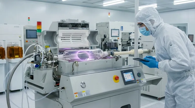
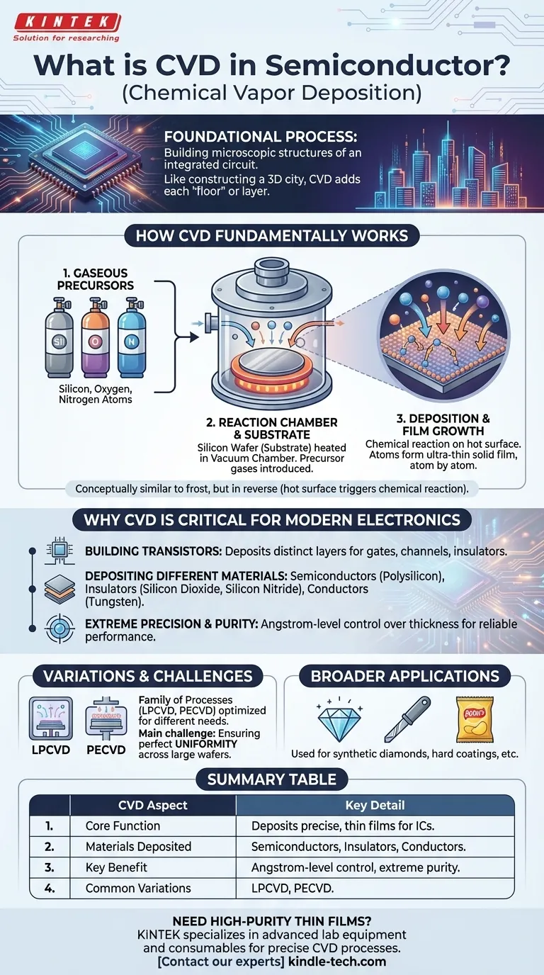
In the semiconductor industry, Chemical Vapor Deposition (CVD) is a foundational process used to build the microscopic structures of an integrated circuit. It works by introducing reactive gases into a chamber, which then decompose and form a high-purity, ultra-thin solid film on the surface of a silicon wafer. These precise layers of material are the essential building blocks for transistors, memory, and processors.
The core challenge in making a computer chip is constructing a three-dimensional city of billions of microscopic components. CVD is the primary method for adding each "floor" or layer to that city, depositing the specific materials—conductors, insulators, and semiconductors—exactly where they are needed.
How CVD Fundamentally Works
At its heart, CVD is a sophisticated way to "grow" a solid material from a gas. The process takes place in a highly controlled environment to ensure the extreme purity and uniformity required for modern electronics.
The Core Principle: Gaseous Precursors
The process begins not with a solid block of material, but with one or more volatile gases known as precursors. These gases contain the atoms (like silicon, oxygen, or nitrogen) that will eventually form the solid film.
The Reaction Chamber and Substrate
A silicon wafer, which acts as the foundation or substrate, is placed inside a vacuum chamber. This chamber is then heated to a specific, often very high, temperature. The precursor gases are precisely metered and introduced into the chamber.
Deposition and Film Growth
On the hot surface of the wafer, a chemical reaction is triggered. The precursor gases react or decompose, leaving behind the desired solid atoms which bond to the wafer surface. Atom by atom, a uniform, solid thin film grows across the entire wafer.
This is conceptually similar to how frost forms on a cold window pane, but in reverse—it relies on a hot surface to trigger a chemical reaction from a gas, rather than a cold surface causing a physical change from a vapor.
Why CVD is Critical for Modern Electronics
Without CVD, the exponential progress of Moore's Law and the creation of powerful, cost-effective devices would be impossible. It is a cornerstone of semiconductor fabrication.
Building Transistors Layer by Layer
A modern microprocessor is a complex, three-dimensional structure. CVD is the technology used to deposit the dozens of distinct layers that form the gates, channels, and insulating barriers of every single transistor on the chip.
Depositing Different Material Types
CVD is not a single-purpose tool. By changing the precursor gases, manufacturers can deposit different types of materials crucial for a circuit's function:
- Semiconductors: Such as polysilicon for transistor gates.
- Insulators (Dielectrics): Such as silicon dioxide or silicon nitride to isolate conductive layers from each other.
- Conductors: Such as tungsten or other metals to form connections.
Enabling Extreme Precision and Purity
The performance of a chip is directly tied to the quality of its material layers. CVD allows for Angstrom-level control over film thickness (an Angstrom is one-tenth of a nanometer) and ensures exceptionally high purity, which is essential for reliable electrical performance.
Understanding the Trade-offs and Variations
While the principle of CVD is straightforward, its implementation is highly complex and involves significant engineering challenges.
It's a Family of Processes
"CVD" is an umbrella term for a family of related technologies, each optimized for different materials and requirements. Variations like Low-Pressure CVD (LPCVD) and Plasma-Enhanced CVD (PECVD) are used to deposit films at different temperatures and rates.
The Challenge of Uniformity
A primary challenge in CVD is ensuring the deposited film has the exact same thickness and properties across the entire surface of the wafer, which can be up to 300mm (12 inches) in diameter. Any variation can lead to failed chips.
Broader Applications Beyond Semiconductors
The same fundamental principle of depositing a durable, high-purity film from a gas is used in many other industries. It is used to create synthetic diamonds, apply hard coatings to cutting tools, and even deposit the thin aluminum layer inside a potato chip bag.
Making the Right Choice for Your Goal
Understanding CVD is about recognizing its role as a fundamental manufacturing primitive. How you apply this knowledge depends on your specific focus.
- If your primary focus is chip design and fabrication: CVD is the primary construction tool used to translate your circuit schematic into a physical, multi-layered device on a wafer.
- If your primary focus is materials science: CVD is a versatile synthesis technique for creating high-purity, crystalline, and amorphous thin films from gaseous reactants.
- If your primary focus is business or technology strategy: CVD is a critical enabling technology whose advancements in precision and cost directly impact the performance, scalability, and economics of the entire digital world.
Grasping this one process is a key step toward understanding how all modern technology is physically built.
Summary Table:
| CVD Aspect | Key Detail |
|---|---|
| Core Function | Deposits precise, thin films on silicon wafers to build integrated circuits. |
| Materials Deposited | Semiconductors (e.g., polysilicon), Insulators (e.g., silicon dioxide), Conductors (e.g., tungsten). |
| Key Benefit | Enables Angstrom-level control and extreme purity for reliable chip performance. |
| Common Variations | LPCVD (Low-Pressure CVD), PECVD (Plasma-Enhanced CVD). |
Need high-purity thin films for your semiconductor or materials research? KINTEK specializes in advanced lab equipment and consumables for precise CVD processes. Our solutions help laboratories achieve the uniformity and purity required for cutting-edge electronics and materials development. Contact our experts today to discuss how we can support your specific fabrication or research goals.
Visual Guide
Related Products
- Chemical Vapor Deposition CVD Equipment System Chamber Slide PECVD Tube Furnace with Liquid Gasifier PECVD Machine
- Customer Made Versatile CVD Tube Furnace Chemical Vapor Deposition Chamber System Equipment
- HFCVD Machine System Equipment for Drawing Die Nano-Diamond Coating
- Split Chamber CVD Tube Furnace with Vacuum Station Chemical Vapor Deposition System Equipment Machine
- Multi Heating Zones CVD Tube Furnace Machine Chemical Vapor Deposition Chamber System Equipment
People Also Ask
- What are the advantages of chemical vapor deposition? Achieve Superior Thin Films for Your Lab
- What are the processes of vapor phase deposition? Understand CVD vs. PVD for Superior Thin Films
- Why is Chemical Vapor Deposition (CVD) equipment uniquely suited for constructing hierarchical superhydrophobic structures?
- What are the core advantages of PE-CVD in OLED encapsulation? Protect Sensitive Layers with Low-Temp Film Deposition
- What is the chemical vapor deposition growth process? Build Superior Thin Films from the Atom Up


